

IEEE Spectrum IEEE Spectrum
-
Video Friday: Silly Robot Dog Jump
by Evan Ackerman on 16. August 2024. at 16:45

Video Friday is your weekly selection of awesome robotics videos, collected by your friends at IEEE Spectrum robotics. We also post a weekly calendar of upcoming robotics events for the next few months. Please send us your events for inclusion.
ICRA@40: 23–26 September 2024, ROTTERDAM, NETHERLANDS
IROS 2024: 14–18 October 2024, ABU DHABI, UAE
ICSR 2024: 23–26 October 2024, ODENSE, DENMARK
Cybathlon 2024: 25–27 October 2024, ZURICH
Enjoy today’s videos!
The title of this video is “Silly Robot Dog Jump” and that’s probably more than you need to know.
[ Deep Robotics ]
It’ll be great when robots are reliably autonomous, but until they get there, collaborative capabilities are a must.
[ Robust AI ]
I am so INCREDIBLY EXCITED for this.
[ IIT Instituto Italiano di Tecnologia ]
In this 3 minutes long one-take video, the LimX Dynamics CL-1 takes on the challenge of continuous heavy objects loading among shelves in a simulated warehouse, showcasing the advantages of the general-purpose form factor of humanoid robots.
[ LimX Dynamics ]
Birds, bats and many insects can tuck their wings against their bodies when at rest and deploy them to power flight. Whereas birds and bats use well-developed pectoral and wing muscles, how insects control their wing deployment and retraction remains unclear because this varies among insect species. Here we demonstrate that rhinoceros beetles can effortlessly deploy their hindwings without necessitating muscular activity. We validated the hypothesis using a flapping microrobot that passively deployed its wings for stable, controlled flight and retracted them neatly upon landing, demonstrating a simple, yet effective, approach to the design of insect-like flying micromachines.
[ Nature ]
Agility Robotics’ CTO, Pras Velagapudi, talks about data collection, and specifically about the different kinds we collect from our real-world robot deployments and generally what that data is used for.
[ Agility Robotics ]
Robots that try really hard but are bad at things are utterly charming.
[ University of Tokyo JSK Lab ]
The DARPA Triage Challenge unsurprisingly has a bunch of robots in it.
[ DARPA ]
The Cobalt security robot has been around for a while, but I have to say, the design really holds up—it’s a good looking robot.
[ Cobalt AI ]
All robots that enter elevators should be programmed to gently sway back and forth to the elevator music. Even if there’s no elevator music.
[ Somatic ]
ABB Robotics and the Texas Children’s Hospital have developed a groundbreaking lab automation solution using ABB’s YuMi® cobot to transfer fruit flies (Drosophila melanogaster) used in the study for developing new drugs for neurological conditions such as Alzheimer’s, Huntington’s and Parkinson’s.
[ ABB ]
Extend Robotics are building embodied AI enabling highly flexible automation for real-world physical tasks. The system features intuitive immersive interface enabling tele-operation, supervision and training AI models.
[ Extend Robotics ]
The recorded livestream of RSS 2024 is now online, in case you missed anything.
[ RSS 2024 ]
-
IEEE and Keysight Team Up to Teach Kids About Electronics
by Robert Schneider on 15. August 2024. at 18:00

IEEE TryEngineering has partnered with Keysight Technologies to develop lesson plans focused on electronics and power simulation. Keysight provides hardware, software, and services to a wide variety of industries, particularly in the area of electronic measurement.
IEEE TryEngineering, an IEEE Educational Activities program, empowers educators to foster the next generation of technology innovators through free, online access to culturally relevant, developmentally appropriate, and educationally sound instructional resources for teachers and community volunteers.
The lesson plans cover a variety of STEM topics, experience levels, and age ranges. Educators should be able to find an applicable topic for their students, regardless of their grade level or interests.
Lesson plans on circuits
There are already a number of lesson plans available through the Keysight partnership that introduce students to electrical concepts, with more being developed. The most popular one thus far is Series and Parallel Circuits, which has been viewed more than 100 times each month. Teams of pupils predict the difference between a parallel and serial circuit design by building examples using wires, light bulbs, and batteries.
“TryEngineering is proud to be Keysight’s partner in attaining the ambitious goal of bringing engineering lessons to 1 million students in 2024.” —Debra Gulick
The newest of the Keysight-sponsored lesson plans, Light Up Name Badge, teaches the basics of circuitry, such as the components of a circuit, series and parallel circuits, and electronic component symbols. Students can apply their newfound knowledge in a design challenge wherein they create a light-up badge with their name.
Developing a workforce through STEM outreach
“Keysight’s commitment to workforce development through preuniversity STEM outreach makes it an ideal partner for IEEE TryEngineering,” says Debra Gulick, director of student and academic education programs for IEEE Educational Activities.
In addition, Keysight’s corporate social responsibility vision to build a better planet by accelerating innovation to connect and secure the world while employing a global business framework of ethical, environmentally sustainable, and socially responsible operations makes it a suitable IEEE partner.
“TryEngineering is proud to be Keysight’s partner in attaining the ambitious goal of bringing engineering lessons to 1 million students in 2024,” Gulick says.
The IEEE STEM Summit, a three-day virtual event in October for IEEE volunteers and educators, is expected to include a session highlighting Keysight’s lesson plans.
Educators and volunteers engaged in outreach activities with students can learn more on the Keysight TryEngineering partnership page.
The arrangement with Keysight was made possible with support from the IEEE Foundation. -
Optical Metasurfaces Shine a Light on Li-Fi, Lidar
by Margo Anderson on 15. August 2024. at 14:00

A new, tunable smart surface can transform a single pulse of light into multiple beams, each aimed in different directions. The proof-of-principle development opens the door to a range of innovations in communications, imaging, sensing, and medicine.
The research comes out of the Caltech lab of Harry Atwater, a professor of applied physics and materials science, and is possible due to a type of nano-engineered material called a metasurface. “These are artificially designed surfaces which basically consist of nanostructured patterns,” says Prachi Thureja, a graduate student in Atwater’s group. “So it’s an array of nanostructures, and each nanostructure essentially allows us to locally control the properties of light.”
The surface can be reconfigured up to millions of times per second to change how it is locally controlling light. That’s rapid enough to manipulate and redirect light for applications in optical data transmission such as optical space communications and Li-Fi, as well as lidar.
“[The metasurface] brings unprecedented freedom in controlling light,” says Alex M.H. Wong, an associate professor of electrical engineering at the City University of Hong Kong. “The ability to do this means one can migrate existing wireless technologies into the optical regime. Li-Fi and LIDAR serve as prime examples.”
Metasurfaces remove the need for lenses and mirrors
Manipulating and redirecting beams of light typically involves a range of conventional lenses and mirrors. These lenses and mirrors might be microscopic in size, but they’re still using optical properties of materials like Snell’s Law, which describes the progress of a wavefront through different materials and how that wavefront is redirected—or refracted—according to the properties of the material itself.
By contrast, the new work offers the prospect of electrically manipulating a material’s optical properties via a semiconducting material. Combined with nano-scaled mirror elements, the flat, microscopic devices can be made to behave like a lens, without requiring lengths of curved or bent glass. And the new metasurface’s optical properties can be switched millions of times per second using electrical signals.
“The difference with our device is by applying different voltages across the device, we can change the profile of light coming off of the mirror, even though physically it’s not moving,” says paper co-author Jared Sisler—also a graduate student in Atwater’s group. “And then we can steer the light like it’s an electrically reprogrammable mirror.”
The device itself, a chip that measures 120 micrometers on each side, achieves its light-manipulating capabilities with an embedded surface of tiny gold antennas in a semiconductor layer of indium tin oxide. Manipulating the voltages across the semiconductor alters the material’s capacity to bend light—also known as its index of refraction. Between the reflection of the gold mirror elements and the tunable refractive capacity of the semiconductor, a lot of rapidly-tunable light manipulation becomes possible.
“I think the whole idea of using a solid-state metasurface or optical device to steer light in space and also use that for encoding information—I mean, there’s nothing like that that exists right now,” Sisler says. “So I mean, technically, you can send more information if you can achieve higher modulation rates. But since it’s kind of a new domain, the performance of our device is more just to show the principle.”
Metasurfaces open up plenty of new possibilities
The principle, says Wong, suggests a wide array of future technologies on the back of what he says are likely near-term metasurface developments and discoveries.
“The metasurface [can] be flat, ultrathin, and lightweight while it attains the functions normally achieved by a series of carefully curved lenses,” Wong says. “Scientists are currently still unlocking the vast possibilities the metasurface has available to us.
“With improvements in nanofabrication, elements with small feature sizes much smaller than the wavelength are now reliably fabricable,” Wong continues. “Many functionalities of the metasurface are being routinely demonstrated, benefiting not just communication but also imaging, sensing, and medicine, among other fields... I know that in addition to interest from academia, various players from industry are also deeply interested and making sizable investments in pushing this technology toward commercialization.”
-
NIST Announces Post-Quantum Cryptography Standards
by Dina Genkina on 13. August 2024. at 10:01

Today, almost all data on the Internet, including bank transactions, medical records, and secure chats, is protected with an encryption scheme called RSA (named after its creators Rivest, Shamir, and Adleman). This scheme is based on a simple fact—it is virtually impossible to calculate the prime factors of a large number in a reasonable amount of time, even on the world’s most powerful supercomputer. Unfortunately, large quantum computers, if and when they are built, would find this task a breeze, thus undermining the security of the entire Internet.
Luckily, quantum computers are only better than classical ones at a select class of problems, and there are plenty of encryption schemes where quantum computers don’t offer any advantage. Today, the U.S. National Institute of Standards and Technology (NIST) announced the standardization of three post-quantum cryptography encryption schemes. With these standards in hand, NIST is encouraging computer system administrators to begin transitioning to post-quantum security as soon as possible.
“Now our task is to replace the protocol in every device, which is not an easy task.” —Lily Chen, NIST
These standards are likely to be a big element of the Internet’s future. NIST’s previous cryptography standards, developed in the 1970s, are used in almost all devices, including Internet routers, phones, and laptops, says Lily Chen, head of the cryptography group at NIST who lead the standardization process. But adoption will not happen overnight.
“Today, public key cryptography is used everywhere in every device,” Chen says. “Now our task is to replace the protocol in every device, which is not an easy task.”
Why we need post-quantum cryptography now
Most experts believe large-scale quantum computers won’t be built for at least another decade. So why is NIST worried about this now? There are two main reasons.
First, many devices that use RSA security, like cars and some IoT devices, are expected to remain in use for at least a decade. So they need to be equipped with quantum-safe cryptography before they are released into the field.
“For us, it’s not an option to just wait and see what happens. We want to be ready and implement solutions as soon as possible.” —Richard Marty, LGT Financial Services
Second, a nefarious individual could potentially download and store encrypted data today, and decrypt it once a large enough quantum computer comes online. This concept is called “harvest now, decrypt later“ and by its nature, it poses a threat to sensitive data now, even if that data can only be cracked in the future.
Security experts in various industries are starting to take the threat of quantum computers seriously, says Joost Renes, principal security architect and cryptographer at NXP Semiconductors. “Back in 2017, 2018, people would ask ‘What’s a quantum computer?’” Renes says. “Now, they’re asking ‘When will the PQC standards come out and which one should we implement?’”
Richard Marty, chief technology officer at LGT Financial Services, agrees. “For us, it’s not an option to just wait and see what happens. We want to be ready and implement solutions as soon as possible, to avoid harvest now and decrypt later.”
NIST’s competition for the best quantum-safe algorithm
NIST announced a public competition for the best PQC algorithm back in 2016. They received a whopping 82 submissions from teams in 25 different countries. Since then, NIST has gone through 4 elimination rounds, finally whittling the pool down to four algorithms in 2022.
This lengthy process was a community-wide effort, with NIST taking input from the cryptographic research community, industry, and government stakeholders. “Industry has provided very valuable feedback,” says NIST’s Chen.
These four winning algorithms had intense-sounding names: CRYSTALS-Kyber, CRYSTALS-Dilithium, Sphincs+, and FALCON. Sadly, the names did not survive standardization: The algorithms are now known as Federal Information Processing Standard (FIPS) 203 through 206. FIPS 203, 204, and 205 are the focus of today’s announcement from NIST. FIPS 206, the algorithm previously known as FALCON, is expected to be standardized in late 2024.
The algorithms fall into two categories: general encryption, used to protect information transferred via a public network, and digital signature, used to authenticate individuals. Digital signatures are essential for preventing malware attacks, says Chen.
Every cryptography protocol is based on a math problem that’s hard to solve but easy to check once you have the correct answer. For RSA, it’s factoring large numbers into two primes—it’s hard to figure out what those two primes are (for a classical computer), but once you have one it’s straightforward to divide and get the other.
“We have a few instances of [PQC], but for a full transition, I couldn’t give you a number, but there’s a lot to do.” —Richard Marty, LGT Financial Services
Two out of the three schemes already standardized by NIST, FIPS 203 and FIPS 204 (as well as the upcoming FIPS 206), are based on another hard problem, called lattice cryptography. Lattice cryptography rests on the tricky problem of finding the lowest common multiple among a set of numbers. Usually, this is implemented in many dimensions, or on a lattice, where the least common multiple is a vector.
The third standardized scheme, FIPS 205, is based on hash functions—in other words, converting a message to an encrypted string that’s difficult to reverse
The standards include the encryption algorithms’ computer code, instructions for how to implement it, and intended uses. There are three levels of security for each protocol, designed to future-proof the standards in case some weaknesses or vulnerabilities are found in the algorithms.
Lattice cryptography survives alarms over vulnerabilities
Earlier this year, a pre-print published to the arXiv alarmed the PQC community. The paper, authored by Yilei Chen of Tsinghua University in Beijing, claimed to show that lattice-based cryptography, the basis of two out of the three NIST protocols, was not, in fact, immune to quantum attacks. On further inspection, Yilei Chen’s argument turned out to have a flaw—and lattice cryptography is still believed to be secure against quantum attacks.
On the one hand, this incident highlights the central problem at the heart of all cryptography schemes: There is no proof that any of the math problems the schemes are based on are actually “hard.” The only proof, even for the standard RSA algorithms, is that people have been trying to break the encryption for a long time, and have all failed. Since post-quantum cryptography standards, including lattice cryptogrphay, are newer, there is less certainty that no one will find a way to break them.
That said, the failure of this latest attempt only builds on the algorithm’s credibility. The flaw in the paper’s argument was discovered within a week, signaling that there is an active community of experts working on this problem. “The result of that paper is not valid, that means the pedigree of the lattice-based cryptography is still secure,” says NIST’s Lily Chen (no relation to Tsinghua University’s Yilei Chen). “People have tried hard to break this algorithm. A lot of people are trying, they try very hard, and this actually gives us confidence.”
NIST’s announcement is exciting, but the work of transitioning all devices to the new standards has only just begun. It is going to take time, and money, to fully protect the world from the threat of future quantum computers.
“We’ve spent 18 months on the transition and spent about half a million dollars on it,” says Marty of LGT Financial Services. “We have a few instances of [PQC], but for a full transition, I couldn’t give you a number, but there’s a lot to do.”
-
Level Up Your Leadership Skills with IEEE Courses
by Nicholas Spada on 12. August 2024. at 19:00

Author and leadership expert John C. Maxwell famously said, “The single biggest way to impact an organization is to focus on leadership development. There is almost no limit to the potential of an organization that recruits good people, raises them up as leaders, and continually develops them.”
Experts confirm that there are clear benefits to fostering leadership by encouraging employees’ professional growth and nurturing and developing company leaders. A culture of leadership development and innovation boosts employee engagement by 20 percent to 25 percent, according to an analysis in the Journal of Applied Psychology. Companies are 22 percent more profitable, on average, when they engage their employees by building a culture of leadership, innovation, and recognition, according to Zippia research.
Developing professionals into strong leaders can have a lasting impact on a company, and the IEEE Professional Development Suite can help make it possible. The training programs in the suite help aspiring technology leaders who want to develop their essential business and management skills. Programs include IEEE Leading Technical Teams, the IEEE | Rutgers Online Mini-MBA for Engineers and Technical Professionals, and the Intensive Wireless Communications and Advanced Topics in Wireless courses offered by the IEEE Communications Society. IEEE also offers topical courses through its eLearning Library.
Tips for leading teams
IEEE Leading Technical Teams is a live, six-hour course offered both in person and virtually. Addressing challenges that come with leading groups, it is designed for team leaders, managers, and directors of engineering and technical teams.
“Participating benefited me and my employer by enhancing my leadership skills in inspiring others to achieve the goals of our organization,” says Stephen Wilkowski, a system test engineer at CACI International in Reston, Va., who completed the training. “I found the leadership practices assessment to be very valuable, as I appreciated the anonymous feedback received from those who I work with. I would recommend the training to anyone desiring to improve their leadership skills.”
Attendees participate in the 360° Leadership Practices Inventory, a tool that solicits confidential feedback on the participant’s strengths and opportunities for improvement from their team members and managers. The program encompasses instructor-led exercises and case studies demonstrating the application of best practices to workplace challenges.
Participants learn the “five practices of exemplary leadership” and receive valuable peer coaching.
To learn more about in-person and virtual options for individuals and companies, complete this form.
A mini-MBA for technologists
The 12-week IEEE | Rutgers Online Mini-MBA for Engineers and Technical Professionals program covers business strategy, new product development management, financial analysis, sales and marketing, and leadership. It includes a combination of expert instruction, peer interaction, self-paced video lessons, interactive assessments, live office hours, and hands-on capstone project experience. The program offers flexible learning opportunities for individual learners as well as customized company cohort options.
Developing professionals into strong leaders can have a lasting impact on a company, and the IEEE Professional Development Suite can help make that possible.
“The mini-MBA was a great opportunity to explore other areas of business that I don’t typically encounter,” says graduate Jonathan Bentz, a senior manager at Nvidia. “I have a customer-facing technical role, and the mini-MBA allowed me to get a taste of the full realm of business leadership.”
For more information, see IEEE | Rutgers Online Mini-MBA for Engineers and Technical Professionals.
Training on wireless communications
The Intensive Wireless Communications and the Advanced Topics in Wireless course series are exclusively presented by the IEEE Communications Society.
The Intensive Wireless interactive live course provides training necessary to stay on top of key developments in the dynamic, rapidly evolving communications industry. Designed for those with an engineering background who want to enhance their knowledge of wireless communication technologies, the series is an ideal way to train individual employees or your entire team at once.
The Advanced Topics in Wireless series is for engineers and technical professionals with a working knowledge of wireless who are looking to enhance their skill set. The series dives into recent advancements, applications, and use cases in emerging connectivity.
Participants in the live, online course series develop a comprehensive view of 5G/NR technology, as well as an understanding of the implementation of all the ITU-specified use case categories such as enhanced mobile broadband, mIoT, and ultra-reliable low-latency communication. The series also provides a robust foundation on the network architecture and the evolution of technology, which enables fully open radio access networks.
Learn more about the Advanced Topics in Wireless Course Series by completing this form.
Topics in the eLearning Library
Tailored for professionals, faculty, and students, the IEEE eLearning Library taps into a wealth of expertise from the organization’s global network of more than 450,000 industry and academia members. Courses cover a wide variety of disciplines including artificial intelligence, blockchain technology, cyber and data security, power and energy, telecommunications, and IEEE standards.
You can help foster growth and leadership skills for your organization by offering employees access to hundreds of courses. Start exploring the library by filling out this form.
Completion of course programs offers learners the ability to earn IEEE certificates bearing professional development hours, continuing education units, and digital badges.
-
Amazon Vies for Nuclear-Powered Data Center
by Andrew Moseman on 12. August 2024. at 18:36

When Amazon Web Services paid US $650 million in March for another data center to add to its armada, the tech giant thought it was buying a steady supply of nuclear energy to power it, too. The Susquehanna Steam Electric Station outside of Berick, Pennsylvania, which generates 2.5 gigawatts of nuclear power, sits adjacent to the humming data center and had been directly powering it since the center opened in 2023.
After striking the deal, Amazon wanted to change the terms of its original agreement to buy 180 megawatts of additional power directly from the nuclear plant. Susquehanna agreed to sell it. But third parties weren’t happy about that, and their deal has become bogged down in a regulatory battle that will likely set a precedent for data centers, cryptocurrency mining operations, and other computing facilities with voracious appetites for clean electricity.
Putting a data center right next to a power plant so that it can draw electricity from it directly, rather than from the grid, is becoming more common as data centers seek out cheap, steady, carbon-free power. Proposals for co-locating data centers next to nuclear power have popped up in New Jersey, Texas, Ohio, and elsewhere. Sweden is considering using small modular reactors to power future data centers.
However, co-location raises questions about equity and energy security, because directly-connected data centers can avoid paying fees that would otherwise help maintain grids. They also hog hundreds of megawatts that could be going elsewhere.
“They’re effectively going behind the meter and taking that capacity off of the grid that would otherwise serve all customers,” says Tony Clark, a senior advisor at the law firm Wilkinson Barker Knauer and a former commissioner at the Federal Energy Regulatory Commission (FERC), who has testified to a U.S. House subcommittee on the subject.
Amazon’s nuclear power deal meets hurdles
The dust-up over the Amazon-Susquehanna agreement started in June, after Amazon subsidiary Amazon Web Services filed a notice to change its interconnection service agreement (ISA) in order to buy more nuclear power from Susquehanna’s parent company, Talen Energy. Amazon wanted to increase the amount of behind-the-meter power it buys from the plant from 300 MW to 480 MW. Shortly after it requested the change, utility giants Exelon and American Electric Power (AEP), filed a protest against the agreement and asked FERC to hold a hearing on the matter.
Their complaint: the deal between Amazon and the nuclear plant would hurt a third party, namely all the customers who buy power from AEP or Exelon utilities. The protest document argues that the arrangement would shift up to $140 million in extra costs onto the people of Pennsylvania, New Jersey, and other states served by PJM, a regional transmission organization that oversees the grid in those areas. “Multiplied by the many similar projects on the drawing board, it is apparent that this unsupported filing has huge financial consequences that should not be imposed on ratepayers without sufficient process to determine and evaluate what is really going on,” their complaint says.
Susquehanna dismissed the argument, effectively saying that its deal with Amazon is none of AEP and Exelon’s business. “It is an unlawful attempt to hijack this limited [ISA] amendment proceeding that they have no stake in and turn it into an ad hoc national referendum on the future of data center load,” Susquehanna’s statement said. (AEP, Exelon, Talen/Susquehanna, and Amazon all declined to comment for this story.)
More disputes like this will likely follow as more data centers co-locate with clean energy. Kevin Schneider, a power system expert at Pacific Northwest National Laboratory and research professor at Washington State University, says it’s only natural that data center operators want the constant, consistent nature of nuclear power. “If you look at the base load nature of nuclear, you basically run it up to a power level and leave it there. It can be well aligned with a server farm.”
Data center operators are also exploring energy options from solar and wind, but these energy sources would have a difficult time matching the constancy of nuclear, even with grid storage to help even out their supply. So giant tech firms look to nuclear to keep their servers running without burning fossil fuels, and use that to trumpet their carbon-free achievements, as Amazon did when it bought the data center in Pennsylvania. “Whether you’re talking about Google or Apple or Microsoft or any of those companies, they tend to have corporate sustainability goals. Being served by a nuclear unit looks great on their corporate carbon balance sheet,” Clark says.
Costs of data centers seeking nuclear energy
Yet such arrangements could have major consequences for other energy customers, Clark argues. For one, directing all the energy from a nuclear plant to a data center is, fundamentally, no different than retiring that plant and taking it offline. “It’s just a huge chunk of capacity leaving the system,” he says, resulting in higher prices and less energy supply for everyone else.
Another issue is the “behind-the-meter” aspect of these kinds of deals. A data center could just connect to the grid and draw from the same supply as everyone else, Clark says. But by connecting directly to the power plant, the center’s owner avoids paying the administrative fees that are used to maintain the grid and grow its infrastructure. Those costs could then get passed on to businesses and residents who have to buy power from the grid. “There’s just a whole list of charges that get assessed through the network service that if you don’t connect through the network, you don’t have to pay,” Clark says. “And those charges are the part of the bill that will go up” for everyone else.
Even the “carbon-free” public relations talking points that come with co-location may be suspect in some cases. In Washington State, where Schneider works, new data centers are being planted next to the region’s abundant hydropower stations, and they’re using so much of that energy that parts of the state are considering adding more fossil fuel capacity to make ends meet. This results in a “zero-emissions shell game,” Clark wrote in a white paper on the subject.
These early cases are likely only the beginning. A report posted in May from the Electric Power Research Institute predicts energy demand from data centers will double by 2030, a leap driven by the fact that AI queries need ten times more energy than traditional internet searches. The International Energy Agency puts the timeline for doubling sooner–in 2026. Data centers, AI, and the cryptocurrency sector consumed an estimated 460 terawatt-hours (TWh) in 2022, and could reach more than 1000 TWh in 2026, the agency predicts.
Data centers face energy supply challenges
New data centers can be built in a matter of months, but it takes years to build utility-scale power projects, says Poorvi Patel, manager of strategic insights at Electric Power Research Institute and contributor to the report. The potential for unsustainable growth in electricity needs has put grid operators on alert, and in some cases has sent them sounding the alarm. Eirgrid, a state-owned transmission operator in Ireland, last week warned of a “mass exodus” of data centers in Ireland if it can’t connect new sources of energy.
There’s only so much existing nuclear power to go around, and enormous logistical and regulatory roadblocks to building more. So data center operators and tech giants are looking for creative solutions. Some are considering small modular reactors (SMRs)–which are advanced nuclear reactors with much smaller operating capacities than conventional reactors. Nano Nuclear Energy, which is developing microreactors–a particularly small type of SMR–last month announced an agreement with Blockfusion to explore the possibility of powering a currently defunct cryptomining facility in Niagara Falls, New York.
“To me, it does seem like a space where, if big tech has a voracious electric power needs and they really want that 24/7, carbon-free power, nuclear does seem to be the answer,” Clark says. “They also have the balance sheets to be able to do some of the risk mitigation that might make it attractive to get an SMR up and running.”
-
Photonic Chip Cuts Cost of Hunting Exoplanets
by Rachel Berkowitz on 12. August 2024. at 13:01

At 6.5 meters in diameter, the James Webb Space Telescope’s primary mirror captures more light than any telescope that’s ever been launched from Earth. But not every astronomer has US $10 billion to spend on a space telescope. So to help bring the cost of space-based astronomy down, researchers at the National Research Council of Canada in Ottawa are working on a way to process starlight on a tiny optical chip. Ross Cheriton, a photonics researcher there, and his students built and tested a CubeSat prototype with a new kind of photonic chip. The goal is to lower the barrier to entry for astronomical science using swarms of lower-cost spacecraft.
“We hope to enable smaller space telescopes to do big science using highly compact instrument-on-chips,” Cheriton says, who is also affiliated with the Quantum and Nanotechnology Research Centre in Ottawa.
Photonics integrated circuits (PICs) use light instead of electricity to process information, and they’re in wide use slinging trillions and trillions of bits around data centers. But only recently have astronomers begun to examine how to use them to push the boundaries of what can be learned about the universe.
Ground-based telescopes are plagued by Earth’s atmosphere, where turbulence blurs incoming light, making it difficult to focus it onto a camera chip. In outer space, telescopes can peer at extremely faint objects in non-visible wavelengths without correcting for the impact of turbulence. That’s where Cheriton aims to boldly go with a PIC filter that detects very subtle gas signatures during an exoplanet “eclipse” called a transit.
The main motivation for putting photonic chips in space is to reduce the size, weight, and cost of components, because it can be produced en masse in a semiconductor foundry. “The dream is a purely fiber and chip-based instrument with no other optics,” says Cheriton. Replacing filters, lenses, and mirrors with a chip also improves stability and scalability compared to ordinary optical parts.
CubeSats—inexpensive, small, and standardized satellites—have proved to be a cost-effective way of deploying small instrument payloads. “The compact nature of PICs is a perfect match for CubeSats to study bright exoplanet systems James Webb doesn’t have time to stare at,” says Cheriton.
For a total mission cost of less than $1 million—compared to the Webb’s $10 billion—an eventual CubeSat mission could stare at a star for days to weeks while it waits for a planet to cross the field of view. Then, it would look for slight changes in the star’s spectrum that are associated with how the planet’s atmosphere absorbs light—telltale evidence of gasses of a biological origin.
Smaller spectroscopy
As a proof-of-concept, Cheriton guided a team of undergraduate students who spent eight months designing and integrating a PIC into a custom 3U CubeSat (10 centimeter x 10 cm x 30 cm) platform. Their silicon nitride photonic circuit sensor proved itself capable of detecting the absorption signatures of CO2 in incoming light.
In their design, light entering the CubeSat’s collimating lens gets focused into a fiber and then pushed to the photonic chip. It enters an etched set of waveguides that includes a ring resonator. Here, light having a specific set of wavelengths builds in intensity over multiple trips around the ring, and is then output to a detector. Because only a select few wavelengths constructively interfere—those chosen to match a gas’s absorption spectrum—the ring serves as a comb-like filter. After the light goes through the ring resonator, the signal from the waveguide gets passed to an output fiber and onto a camera connected to a Raspberry Pi computer for processing. A single pixel’s intensity therefore serves as a reading for a gas’s presence.
 Light travels through a waveguide on a photonic integrated circuit.Teseract
Because it’s built on a chip, the sensor could be multiplexed for observing several objects or sense different gasses simultaneously. Additionally, all the light falling on a single pixel means that the signal is more sensitive than a traditional spectrometer, says Cheriton. Moreover, instead of hunting for peaks in a full spectrum, the technology looks for how well the absorption spectrum matches that of a specific gas, a more efficient process. “If something is in space, you don’t want to send gigabytes of data home if you don’t have to,” he says.
Space travel is still a long way off for the astrophotonic CubeSat. The current design does not use space-qualified components. But Cheriton’s students tested it in the lab for red light (635 nm) and CO2 in a gas cell. They used a “ground station” computer to transmit all commands and receive all results—and to monitor the photovoltaics and collect data from the flight control sensors onboard their CubeSat.
Next, the team plans to test whether their sensor can detect oxygen with the silicon nitride chip, a material that was chosen for its transparency to the gas’s 760 nm wavelength. Success would leave them well positioned to meet what Cheriton calls the next huge milestone for astronomers: looking for an earth-like planet with oxygen.
The work was presented at the Optica (formerly Optical Society of America) Advanced Photonics conference in July.
-
Hybrid Bonding Plays Starring Role in 3D Chips
by Samuel K. Moore on 11. August 2024. at 13:00

Chipmakers continue to claw for every spare nanometer to continue scaling down circuits, but a technology involving things that are much bigger—hundreds or thousands of nanometers across—could be just as significant over the next five years.
Called hybrid bonding, that technology stacks two or more chips atop one another in the same package. That allows chipmakers to increase the number of transistors in their processors and memories despite a general slowdown in the shrinking of transistors, which once drove Moore’s Law. At the IEEE Electronic Components and Technology Conference (ECTC) this past May in Denver, research groups from around the world unveiled a variety of hard-fought improvements to the technology, with a few showing results that could lead to a record density of connections between 3D stacked chips: some 7 million links per square millimeter of silicon.
All those connections are needed because of the new nature of progress in semiconductors, Intel’s Yi Shi told engineers at ECTC. Moore’s Law is now governed by a concept called system technology co-optimization, or STCO, whereby a chip’s functions, such as cache memory, input/output, and logic, are fabricated separately using the best manufacturing technology for each. Hybrid bonding and other advanced packaging tech can then be used to assemble these subsystems so that they work every bit as well as a single piece of silicon. But that can happen only when there’s a high density of connections that can shuttle bits between the separate pieces of silicon with little delay or energy consumption.
Out of all the advanced-packaging technologies, hybrid bonding provides the highest density of vertical connections. Consequently, it is the fastest growing segment of the advanced-packaging industry, says Gabriella Pereira, technology and market analyst at Yole Group. The overall market is set to more than triple to US $38 billion by 2029, according to Yole, which projects that hybrid bonding will make up about half the market by then, although today it’s just a small portion.
In hybrid bonding, copper pads are built on the top face of each chip. The copper is surrounded by insulation, usually silicon oxide, and the pads themselves are slightly recessed from the surface of the insulation. After the oxide is chemically modified, the two chips are then pressed together face-to-face, so that the recessed pads on each align. This sandwich is then slowly heated, causing the copper to expand across the gap and fuse, connecting the two chips.
Making Hybrid Bonding Better

- Hybrid bonding starts with two wafers or a chip and a wafer facing each other. The mating surfaces are covered in oxide insulation and slightly recessed copper pads connected to the chips’ interconnect layers.
- The wafers are pressed together to form an initial bond between the oxides.
- The stacked wafers are then heated slowly, strongly linking the oxides and expanding the copper to form an electrical connection.
- To form more secure bonds, engineers are flattening the last few nanometers of oxide. Even slight bulges or warping can break dense connections.
- The copper must be recessed from the surface of the oxide just the right amount. Too much and it will fail to form a connection. Too little and it will push the wafers apart. Researchers are working on ways to control the level of copper down to single atomic layers.
- The initial links between the wafers are weak hydrogen bonds. After annealing, the links are strong covalent bonds [below]. Researchers expect that using different types of surfaces, such as silicon carbonitride, which has more locations to form chemical bonds, will lead to stronger links between the wafers.
- The final step in hybrid bonding can take hours and require high temperatures. Researchers hope to lower the temperature and shorten the process time.
- Although the copper from both wafers presses together to form an electrical connection, the metal’s grain boundaries generally do not cross from one side to the other. Researchers are trying to cause large single grains of copper to form across the boundary to improve conductance and stability.
Hybrid bonding can either attach individual chips of one size to a wafer full of chips of a larger size or bond two full wafers of chips of the same size. Thanks in part to its use in camera chips, the latter process is more mature than the former, Pereira says. For example, engineers at the European microelectronics-research institute Imec have created some of the most dense wafer-on-wafer bonds ever, with a bond-to-bond distance (or pitch) of just 400 nanometers. But Imec managed only a 2-micrometer pitch for chip-on-wafer bonding.
The latter is a huge improvement over the advanced 3D chips in production today, which have connections about 9 μm apart. And it’s an even bigger leap over the predecessor technology: “microbumps” of solder, which have pitches in the tens of micrometers.
“With the equipment available, it’s easier to align wafer to wafer than chip to wafer. Most processes for microelectronics are made for [full] wafers,” says Jean-Charles Souriau, scientific leader in integration and packaging at the French research organization CEA Leti. But it’s chip-on-wafer (or die-to-wafer) that’s making a splash in high-end processors such as those from AMD, where the technique is used to assemble compute cores and cache memory in its advanced CPUs and AI accelerators.
In pushing for tighter and tighter pitches for both scenarios, researchers are focused on making surfaces flatter, getting bound wafers to stick together better, and cutting the time and complexity of the whole process. Getting it right could revolutionize how chips are designed.
WoW, Those Are Some Tight Pitches
The recent wafer-on-wafer (WoW) research that achieved the tightest pitches—from 360 nm to 500 nm—involved a lot of effort on one thing: flatness. To bond two wafers together with 100-nm-level accuracy, the whole wafer has to be nearly perfectly flat. If it’s bowed or warped to the slightest degree, whole sections won’t connect.
Flattening wafers is the job of a process called chemical mechanical planarization, or CMP. It’s essential to chipmaking generally, especially for producing the layers of interconnects above the transistors.
“CMP is a key parameter we have to control for hybrid bonding,” says Souriau. The results presented at ECTC show CMP being taken to another level, not just flattening across the wafer but reducing mere nanometers of roundness on the insulation between the copper pads to ensure better connections.
“It’s difficult to say what the limit will be. Things are moving very fast.” —Jean-Charles Souriau, CEA Leti
Other researchers focused on ensuring those flattened parts stick together strongly enough. They did so by experimenting with different surface materials such as silicon carbonitride instead of silicon oxide and by using different schemes to chemically activate the surface. Initially, when wafers or dies are pressed together, they are held in place with relatively weak hydrogen bonds, and the concern is whether everything will stay in place during further processing steps. After attachment, wafers and chips are then heated slowly, in a process called annealing, to form stronger chemical bonds. Just how strong these bonds are—and even how to figure that out—was the subject of much of the research presented at ECTC.
Part of that final bond strength comes from the copper connections. The annealing step expands the copper across the gap to form a conductive bridge. Controlling the size of that gap is key, explains Samsung’s Seung Ho Hahn. Too little expansion, and the copper won’t fuse. Too much, and the wafers will be pushed apart. It’s a matter of nanometers, and Hahn reported research on a new chemical process that he hopes to use to get it just right by etching away the copper a single atomic layer at a time.
The quality of the connection counts, too. The metals in chip interconnects are not a single crystal; instead they’re made up of many grains, crystals oriented in different directions. Even after the copper expands, the metal’s grain boundaries often don’t cross from one side to another. Such a crossing should reduce a connection’s electrical resistance and boost its reliability. Researchers at Tohoku University in Japan reported a new metallurgical scheme that could finally generate large, single grains of copper that cross the boundary. “This is a drastic change,” says Takafumi Fukushima, an associate professor at Tohoku. “We are now analyzing what underlies it.”
Other experiments discussed at ECTC focused on streamlining the bonding process. Several sought to reduce the annealing temperature needed to form bonds—typically around 300 °C—as to minimize any risk of damage to the chips from the prolonged heating. Researchers from Applied Materials presented progress on a method to radically reduce the time needed for annealing—from hours to just 5 minutes.
CoWs That Are Outstanding in the Field
 Imec used plasma etching to dice up chips and give them chamfered corners. The technique relieves mechanical stress that could interfere with bonding.Imec
Chip-on-wafer (CoW) hybrid bonding is more useful to makers of advanced CPUs and GPUs at the moment: It allows chipmakers to stack chiplets of different sizes and to test each chip before it’s bound to another, ensuring that they aren’t dooming an expensive CPU with a single flawed part.
But CoW comes with all of the difficulties of WoW and fewer of the options to alleviate them. For example, CMP is designed to flatten wafers, not individual dies. Once dies have been cut from their source wafer and tested, there’s less that can be done to improve their readiness for bonding.
Nevertheless, researchers at Intel reported CoW hybrid bonds with a 3-μm pitch, and, as mentioned, a team at Imec managed 2 μm, largely by making the transferred dies very flat while they were still attached to the wafer and keeping them extra clean throughout the process. Both groups used plasma etching to dice up the dies instead of the usual method, which uses a specialized blade. Unlike a blade, plasma etching doesn’t lead to chipping at the edges, which creates debris that could interfere with connections. It also allowed the Imec group to shape the die, making chamfered corners that relieve mechanical stress that could break connections.
CoW hybrid bonding is going to be critical to the future of high-bandwidth memory (HBM), according to several researchers at ECTC. HBM is a stack of DRAM dies—currently 8 to 12 dies high—atop a control-logic chip. Often placed within the same package as high-end GPUs, HBM is crucial to handling the tsunami of data needed to run large language models like ChatGPT. Today, HBM dies are stacked using microbump technology, so there are tiny balls of solder surrounded by an organic filler between each layer.
But with AI pushing memory demand even higher, DRAM makers want to stack 20 layers or more in HBM chips. The volume that microbumps take up means that these stacks will soon be too tall to fit properly in the package with GPUs. Hybrid bonding would shrink the height of HBMs and also make it easier to remove excess heat from the package, because there would be less thermal resistance between its layers.
“I think it’s possible to make a more-than-20-layer stack using this technology.” —Hyeonmin Lee, Samsung
At ECTC, Samsung engineers showed that hybrid bonding could yield a 16-layer HBM stack. “I think it’s possible to make a more-than-20-layer stack using this technology,” says Hyeonmin Lee, a senior engineer at Samsung. Other new CoW technology could also help bring hybrid bonding to high-bandwidth memory. Researchers at CEA Leti are exploring what’s known as self-alignment technology, says Souriau. That would help ensure good CoW connections using just chemical processes. Some parts of each surface would be made hydrophobic and some hydrophilic, resulting in surfaces that would slide into place automatically.
At ECTC, researchers from Tohoku University and Yamaha Robotics reported work on a similar scheme, using the surface tension of water to align 5-μm pads on experimental DRAM chips with better than 50-nm accuracy.
The Bounds of Hybrid Bonding
Researchers will almost certainly keep reducing the pitch of hybrid-bonding connections. A 200-nm WoW pitch is not just possible but desirable, Han-Jong Chia, a project manager for pathfinding systems at Taiwan Semiconductor Manufacturing Co. , told engineers at ECTC. Within two years, TSMC plans to introduce a technology called backside power delivery. (Intel plans the same for the end of this year.) That’s a technology that puts the chip’s chunky power-delivery interconnects below the surface of the silicon instead of above it. With those power conduits out of the way, the uppermost levels can connect better to smaller hybrid-bonding bond pads, TSMC researchers calculate. Backside power delivery with 200-nm bond pads would cut down the capacitance of 3D connections so much that a measure of energy efficiency and signal speed would be as much as eight times better than what can be achieved with 400-nm bond pads.
 Chip-on-wafer hybrid bonding is more useful than wafer-on-wafer bonding, in that it can place dies of one size onto a wafer of larger dies. However, the density of connections that can be achieved is lower than for wafer-on-wafer bonding.Imec
At some point in the future, if bond pitches narrow even further, Chia suggests, it might become practical to “fold” blocks of circuitry so they are built across two wafers. That way some of what are now long connections within the block might be able to take a vertical shortcut, potentially speeding computations and lowering power consumption.
And hybrid bonding may not be limited to silicon. “Today there is a lot of development in silicon-to-silicon wafers, but we are also looking to do hybrid bonding between gallium nitride and silicon wafers and glass wafers…everything on everything,” says CEA Leti’s Souriau. His organization even presented research on hybrid bonding for quantum-computing chips, which involves aligning and bonding superconducting niobium instead of copper.
“It’s difficult to say what the limit will be,” Souriau says. “Things are moving very fast.”
This article was updated on 11 August 2024.
This article appears in the September 2024 print issue.
-
Trailblazing Tech Leader Helps Shape U.S. AI Strategy
by Joanna Goodrich on 10. August 2024. at 13:00

In the two years since Arati Prabhakar was appointed director of the White House Office of Science and Technology Policy, she has set the United States on a course toward regulating artificial intelligence. The IEEE Fellow advised the U.S. President Joe Biden in writing the executive order he issued to accomplish the goal just six months after she began her new role in 2022.
Prabhakar is the first woman and the first person of color to serve as OSTP director, and she has broken through the glass ceiling at other agencies as well. She was the first woman to lead the National Institute of Standards and Technology (NIST) and the Defense Advanced Research Projects Agency.
Arati Prabhakar
Employer
U.S. government
Title
Director of the White House Office of Science and Technology Policy
Member grade
Fellow
Alma maters
Texas Tech University; Caltech
Working in the public sector wasn’t initially on her radar. Not until she became a DARPA program manager in 1986, she says, did she really understand what she could accomplish as a government official.
“What I have come to love about [public service] is the opportunity to shape policies at a scale that is really unparalleled,” she says.
Prabhakar’s passion for tackling societal challenges by developing technology also led her to take leadership positions at companies including Raychem (now part of TE Connectivity), Interval Research Corp., and U.S. Venture Partners. In 2019 she helped found Actuate, a nonprofit in Palo Alto, Calif., that seeks to create technology to help address climate change, data privacy, health care access, and other pressing issues.
“I really treasure having seen science, technology, and innovation from all different perspectives,” she says. “But the part I have loved most is public service because of the impact and reach that it can have.”
Discovering her passion for electrical engineering
Prabhakar, who was born in India and raised in Texas, says she decided to pursue a STEM career because when she was growing up, her classmates said women weren’t supposed to work in science, technology, engineering or mathematics.
“Them saying that just made me want to pursue it more,” she says. Her parents, who had wanted her to become a doctor, supported her pursuit of engineering, she adds.
After earning a bachelor’s degree in electrical engineering in 1979 from Texas Tech University, in Lubbock, she moved to California to continue her education at Caltech. She graduated with a master’s degree in EE in 1980, then earned a doctorate in applied physics in 1984. Her doctoral thesis focused on understanding deep-level defects and impurities in semiconductors that affect device performance.
After acquiring her Ph.D., she says, she wanted to make a bigger impact with her research than academia would allow, so she applied for a policy fellowship from the American Association for the Advancement of Science to work at the congressional Office of Technology Assessment. The office examines issues involving new or expanding technologies, assesses their impact, and studies whether new policies are warranted.
“We have huge aspirations for the future—such as mitigating climate change—that science and technology have to be part of achieving.”
“I wanted to share my research in semiconductor manufacturing processes with others,” Prabhakar says. “That’s what felt exciting and valuable to me.”
She was accepted into the program and moved to Washington, D.C. During the yearlong fellowship, she conducted a study on microelectronics R&D for the research and technology subcommittee of the U.S. House of Representatives committee on science, space, and technology. The subcommittee oversees STEM-related matters including education, policy, and standards.
While there, she worked with people who were passionate about public service and government, but she didn’t feel the same, she says, until she joined DARPA. As program manager, Prabhakar established and led several projects including a microelectronics office that invests in developing new technologies in areas such as lithography, optoelectronics, infrared imaging, and neural networks.
In 1993 an opportunity arose that she couldn’t refuse, she says: President Bill Clinton nominated her to direct the National Institute of Standards and Technology. NIST develops technical guidelines and conducts research to create tools that improve citizens’ quality of life. At age 34, she became the first woman to lead the agency.
Believing in IEEE’s Mission
Like many IEEE members, Prabhakar says, she joined IEEE as a student member while attending Texas Tech University because the organization’s mission aligned with her belief that engineering is about creating value in the world.
She continues to renew her membership, she says, because IEEE emphasizes that technology should benefit humanity.
“It really comes back to this idea of the purpose of engineering and the role that it plays in the world,” she says.
After leading NIST through the first Clinton administration, she left for the private sector, including stints as CTO at appliance-component maker Raychem in Menlo Park, Calif., and president of private R&D lab Interval Research of Palo Alto, Calif. In all, she spent the next 14 years in the private sector, mostly as a partner at U.S. Venture Partners, in Menlo Park, where she invested in semiconductor and clean-tech startups.
In 2012 she returned to DARPA and became its first female director.
“When I received the call offering me the job, I stopped breathing,” Prabhakar says. “It was a once-in-a-lifetime opportunity to make a difference at an agency that I had loved earlier in my career. And it proved to be just as meaningful an experience as I had hoped.”
For the next five years she led the agency, focusing on developing better military systems and the next generation of artificial intelligence, as well as creating solutions in social science, synthetic biology, and neurotechnology.
Under her leadership, in 2014 DARPA established the Biological Technologies Office to oversee basic and applied research in areas including gene editing, neurosciences, and synthetic biology. The office launched the Pandemic Prevention Platform, which helped fund the development of the mRNA technology that is used in the Moderna and Pfizer coronavirus vaccines.
She left the agency in 2017 to move back to California with her family.
“When I left the organization, what was very much on my mind was that the United States has the most powerful innovation engine the world has ever seen,” Prabhakar says. “At the same time, what kept tugging at me was that we have huge aspirations for the future—such as mitigating climate change—that science and technology have to be part of achieving.”
That’s why, in 2019, she helped found Actuate. She served as the nonprofit’s chief executive until 2022, when she took on the role of OSTP director.
Although she didn’t choose her career path because it was her passion, she says, she came to realize that she loves the role that engineering, science, and technology play in the world because of their “power to change how the future unfolds.”

Leading AI regulation worldwide
When Biden asked if Prabhakar would take the OSTP job, she didn’t think twice, she says. “When do you need me to move in?” she says she told him.
“I was so excited to work for the president because he sees science and technology as a necessary part of creating a bright future for the country,” Prabhakar says.
A month after she took office, the generative AI program ChatGPT launched and became a hot topic.
“AI was already being used in different areas, but all of a sudden it became visible to everyone in a way that it really hadn’t been before,” she says.
Regulating AI became a priority for the Biden administration because of the technology’s breadth and power, she says, as well as the rapid pace at which it’s being developed.
Prabhakar led the creation of Biden’s Executive Order on the Safe, Secure, and Trustworthy Development and Use of Artificial Intelligence. Signed on 30 October 2022, the order outlines goals such as protecting consumers and their privacy from AI systems, developing watermarking systems for AI-generated content, and warding off intellectual property theft stemming from the use of generative models.
“The executive order is possibly the most important accomplishment in relation to AI,” Prabhakar says. “It’s a tool that mobilizes the [U.S. government’s] executive branch and recognizes that such systems have safety and security risks, but [it] also enables immense opportunity. The order has put the branches of government on a very constructive path toward regulation.”
Meanwhile, the United States spearheaded a U.N. resolution to make regulating AI an international priority. The United Nations adopted the measure this past March. In addition to defining regulations, it seeks to use AI to advance progress on the U.N.’s sustainable development goals.
“There’s much more to be done,” Prabhakar says, “but I’m really happy to see what the president has been able to accomplish, and really proud that I got to help with that.”
-
Video Friday: The Secrets of Shadow Robot’s New Hand
by Evan Ackerman on 09. August 2024. at 15:30

Video Friday is your weekly selection of awesome robotics videos, collected by your friends at IEEE Spectrum robotics. We also post a weekly calendar of upcoming robotics events for the next few months. Please send us your events for inclusion.
ICRA@40: 23–26 September 2024, ROTTERDAM, NETHERLANDS
IROS 2024: 14–18 October 2024, ABU DHABI, UAE
ICSR 2024: 23–26 October 2024, ODENSE, DENMARK
Cybathlon 2024: 25–27 October 2024, ZURICH
Enjoy today’s videos!
At ICRA 2024, in Tokyo last May, we sat down with the director of Shadow Robot, Rich Walker, to talk about the journey toward developing its newest model. Designed for reinforcement learning, the hand is extremely rugged, has three fingers that act like thumbs, and has fingertips that are highly sensitive to touch.
[ IEEE Spectrum ]
Food Angel is a food delivery robot to help with the problems of food insecurity and homelessness. Utilizing autonomous wheeled robots for this application may seem to be a good approach, especially with a number of successful commercial robotic delivery services. However, besides technical considerations such as range, payload, operation time, autonomy, etc., there are a number of important aspects that still need to be investigated, such as how the general public and the receiving end may feel about using robots for such applications, or human-robot interaction issues such as how to communicate the intent of the robot to the homeless.
[ RoMeLa ]
The UKRI FLF team RoboHike of UCL Computer Science of the Robot Perception and Learning lab with Forestry England demonstrate the ANYmal robot to help preserve the cultural heritage of an historic mine in the Forest of Dean, Gloucestershire, UK.
This clip is from a reboot of the British TV show “Time Team.” If you’re not already a fan of “Time Team,” let me just say that it is one of the greatest retro reality TV shows ever made, where actual archaeologists wander around the United Kingdom and dig stuff up. If they can find anything. Which they often can’t. And also it has Tony Robinson (from “Blackadder”), who runs everywhere for some reason. Go to Time Team Classics on YouTube for 70+ archived episodes.
[ UCL RPL ]
UBTECH humanoid robot Walker S Lite is working in Zeekr’s intelligent factory to complete handling tasks at the loading workstation for 21 consecutive days, and assist its employees with logistics work.
[ UBTECH ]
Current visual navigation systems often treat the environment as static, lacking the ability to adaptively interact with obstacles. This limitation leads to navigation failure when encountering unavoidable obstructions. In response, we introduce IN-Sight, a novel approach to self-supervised path planning, enabling more effective navigation strategies through interaction with obstacles.
[ ETH Zurich paper / IROS 2024 ]
When working on autonomous cars, sometimes it’s best to start small.
[ University of Pennsylvania ]
MIT MechE researchers introduce an approach called SimPLE (Simulation to Pick Localize and placE), a method of precise kitting, or pick and place, in which a robot learns to pick, regrasp, and place objects using the object’s computer-aided design (CAD) model, and all without any prior experience or encounters with the specific objects.
[ MIT ]
Staff, students (and quadruped robots!) from UCL Computer Science wish the Great Britain athletes the best of luck this summer in the Olympic Games & Paralympics.
Walking in tall grass can be hard for robots, because they can’t see the ground that they’re actually stepping on. Here’s a technique to solve that, published in Robotics and Automation Letters last year.
[ ETH Zurich Robotic Systems Lab ]
There is no such thing as excess batter on a corn dog, and there is also no such thing as a defective donut. And apparently, making Kool-Aid drink pouches is harder than it looks.
[ Oxipital AI ]
Unitree has open-sourced its software to teleoperate humanoids in VR for training-data collection.
[ Unitree / GitHub ]
Nothing more satisfying than seeing point-cloud segments wiggle themselves into place, and CSIRO’s Wildcat SLAM does this better than anyone.
[ IEEE Transactions on Robotics ]
A lecture by Mentee Robotics CEO Lior Wolf, on Mentee’s AI approach.
[ Mentee Robotics ]
-
Quantum Cryptography Has Everyone Scrambling
by Margo Anderson on 08. August 2024. at 14:00

While the technology world awaits NIST’s latest “post-quantum” cryptography standards this summer, a parallel effort is underway to also develop cryptosystems that are grounded in quantum technology—what are called quantum-key distribution or QKD systems.
As a result, India, China, and a range of technology organizations in the European Union and United States are researching and developing QKD and weighing standards for the nascent cryptography alternative. And the biggest question of all is how or if QKD fits into a robust, reliable, and fully future-proof cryptography system that will ultimately become the global standard for secure digital communications into the 2030s. As in any emerging technology standard, different players are staking claims on different technologies and implementations of those technologies. And many of the big players are pursuing such divergent options because no technology is a clear winner at the moment.
According to Ciel Qi, a research analyst at the New York-based Rhodium Group, there’s one clear leader in QKD research and development—at least for now. “While China likely holds an advantage in QKD-based cryptography due to its early investment and development, others are catching up,” says Qi.
Two different kinds of “quantum secure” tech
At the center of these varied cryptography efforts is the distinction between QKD and post-quantum cryptography (PQC) systems. QKD is based on quantum physics, which holds that entangled qubits can store their shared information so securely that any effort to uncover it is unavoidably detectable. Sending pairs of entangled-photon qubits to both ends of a network provides the basis for physically secure cryptographic keys that can lock down data packets sent across that network.
Typically, quantum cryptography systems are built around photon sources that chirp out entangled photon pairs—where photon A heading down one length of fiber has a polarization that’s perpendicular to the polarization of photon B heading in the other direction. The recipients of these two photons perform separate measurements that enable both recipients to know that they and only they have the shared information transmitted by these photon pairs. (Otherwise, if a third party had intervened and measured one or both photons first, the delicate photon states would have been irreparably altered before reaching the recipients.)
“People can’t predict theoretically that these PQC algorithms won’t be broken one day.” —Doug Finke, Global Quantum Intelligence
This shared bit the two people on opposite ends of the line have in common then becomes a 0 or 1 in a budding secret key that the two recipients build up by sharing more and more entangled photons. Build up enough shared secret 0s and 1s between sender and receiver, and that secret key can be used for a type of strong cryptography, called a one-time pad, that guarantees a message’s safe transmission and faithful receipt by only the intended recipient.
By contrast, post-quantum cryptography (PQC) is based not around quantum physics but pure math, in which next-generation cryptographic algorithms are designed to run on conventional computers. And it’s the algorithms’ vast complexity that makes PQC security systems practically uncrackable, even by a quantum computer. So NIST—the U.S. National Institute of Standards and Technology—is developing gold-standard PQC systems that will undergird tomorrow’s post-quantum networks and communications.
The big problem with the latter approach, says Doug Finke, chief content officer of the New York-based Global Quantum Intelligence, is PQC is only believed (on very, very good but not infallible evidence) to be uncrackable by a fully-grown quantum computer. PQC, in other words, cannot necessarily offer the ironclad “quantum security” that’s promised.
“People can’t predict theoretically that these PQC algorithms won’t be broken one day,” Finke says. “On the other hand, QKD—there are theoretical arguments based on quantum physics that you can’t break a QKD network.”
That said, real-world QKD implementations might still be hackable via side-channel, device-based, and other clever attacks. Plus, QKD also requires direct access to a quantum-grade fiber optics network and sensitive quantum communications tech, neither of which is exactly commonplace today. “For day-to-day stuff, for me to send my credit card information to Amazon on my cellphone,” Finke says, “I’m not going to use QKD.”
China’s early QKD lead dwindling
According to Qi, China may have originally picked QKD as a focal point of their quantum technology development in part because the U.S. was not directing its efforts that way. “[The] strategic focus on QKD may be driven by China’s desire to secure a unique technological advantage, particularly as the U.S. leads in PQC efforts globally,” she says.
In particular, she points to ramped up efforts to use satellite uplinks and downlinks as the basis for free-space Chinese QKD systems. Citing as a source China’s “father of quantum,” Pan Jianwei, Qi says, “To achieve global quantum network coverage, China is currently developing a medium-high orbit quantum satellite, which is expected to be launched around 2026.”
That said, the limiting factor in all QKD systems to date is their ultimate reliance on a single photon to represent each qubit. Not even the most exquisitely-refined lasers and fiber optic lines can’t escape the vulnerability of individual photons.
QKD repeaters, which would blindly replicate a single photon’s quantum state but not leak any distinguishing information about the individual photons passing through—meaning the repeater would not be hackable by eavesdroppers—do not exist today. But, Finke says, such tech is achievable, though at least 5 to 10 years away. “It definitely is early days,” he says.
“While China likely holds an advantage in QKD-based cryptography due to its early investment and development, others are catching up.” —Ciel Qi, Rhodium Group
“In China they do have a 2,000-kilometer network,” Finke says. “But it uses this thing called trusted nodes. I think they have over 30 in the Beijing to Shanghai network. So maybe every 100 km, they have this unit which basically measures the signal... and then regenerates it. But the trusted node you have to locate on an army base or someplace like that. If someone breaks in there, they can hack into the communications.”
Meanwhile, India has been playing catch-up, according to Satyam Priyadarshy, a senior advisor to Global Quantum Intelligence. Priyadarshy says India’s National Quantum Mission includes plans for QKD communications research—aiming ultimately for QKD networks connecting cities over 2,000-km distances, as well as across similarly long-ranging satellite communications networks.
Priyadarshy points both to government QKD research efforts—including at the Indian Space Research Organization—and private enterprise-based R&D, including by the Bengaluru-based cybersecurity firm QuNu Labs. Priyadarshy says that QuNu, for example, has been working on a hub-and-spoke framework named ChaQra for QKD. (Spectrum also sent requests for comment to officials at India’s Department of Telecommunications, which were unanswered as of press time.)
“A hybrid of QKD and PQC is the most likely solution for a quantum safe network.” —Satyam Priyadarshy, Global Quantum Intelligence
In the U.S. and European Union, similar early-stage efforts are also afoot. Contacted by IEEE Spectrum, officials from the European Telecommunications Standards Institute (ETSI); the International Standards Organization (ISO); the International Electrotechnical Commission (IEC); and the IEEE Communications Society confirmed initiatives and working groups that are now working to both promote QKD technologies and emergent standards now taking shape.
“While ETSI is fortunate to have experts in a broad range of relevant topics, there is a lot to do,” says Martin Ward, senior research scientist based at Toshiba’s Cambridge Research Laboratory in England, and chair of a QKD industry standards group at ETSI.
Multiple sources contacted for this article envisioned a probable future in which PQC will likely be the default standard for most secure communications in a world of pervasive quantum computing. Yet, PQC also cannot avoid its potential Achilles’ heel against increasingly powerful quantum algorithms and machines either. This is where, the sources suggest, QKD could offer the prospect of hybrid secure communications that PQC alone could never provide.
“QKD provides [theoretical] information security, while PQC enables scalab[ility],” Priyadarshy says. “A hybrid of QKD and PQC is the most likely solution for a quantum safe network.” But he added that efforts at investigating hybrid QKD-PQC technologies and standards today are “very limited.”
Then, says Finke, QKD could still have the final say, even in a world where PQC remains preeminent. Developing QKD technology just happens, he points out, to also provide the basis for a future quantum Internet.
“It’s very important to understand that QKD is actually just one use case for a full quantum network,” Finke says.
“There’s a lot of applications, like distributed quantum computing and quantum data centers and quantum sensor networks,” Finke adds. “So even the research that people are doing now in QKD is still very, very helpful because a lot of that same technology can be leveraged for some of these other use cases.”
-
A Non-Engineer’s Journey to IEEE Leadership
by Kathy Pretz on 07. August 2024. at 18:00

Sharlene Brown often accompanied her husband, IEEE Senior Member Damith Wickramanayake, to organization meetings. He has held leadership positions in the IEEE Jamaica Section, in IEEE Region 3, and on the IEEE Member and Geographic Activities board. Both are from Jamaica.
She either waited outside the conference room or helped with tasks such as serving refreshments. Even though her husband encouraged her to sit in on the meetings, she says, she felt uncomfortable doing so because she wasn’t an engineer. Brown is an accountant and human resources professional. Her husband is a computer science professor at the University of Technology, Jamaica, in Kingston. He is currently Region 3’s education activities coordinator and a member of the section’s education and outreach committee for the IEEE Educational Activities Board.
Sharlene Brown
Employer
Maritime Authority of Jamaica, in Kingston
Title
Assistant accountant
Member grade
Senior member
Alma mater
University of Technology, Jamaica, in Kingston; Tsinghua University, in Beijing
After earning her master’s degree in public administration in 2017, Brown says, she felt she finally was qualified to join IEEE, so she applied. Membership is open to individuals who, by education or experience, are competent in different fields including management. She was approved the same year.
“When I joined IEEE, I would spend long hours at night reading various operations manuals and policies because I wanted to know what I was getting into,” she says. “I was always learning. That’s how I got to know a lot of things about the organization.”
Brown is now a senior member and an active IEEE volunteer. She founded the Jamaica Section’s Women in Engineering group; established a student branch; sits on several high-level IEEE boards; and ran several successful recruitment campaigns to increase the number of senior members in Jamaica and throughout Region 3.
Brown was also a member of the subcommittee of the global Women in Engineering committee; she served as membership coordinator and ran several successful senior member campaigns, elevating women on the committee and across IEEE.
Brown also was integral in the promotion and follow-up activities for the One IEEE event held in January at the University of Technology, Jamaica. The first-of-its-kind workshop connected more than 200 participants to each other and to the organization by showcasing Jamaica’s active engineering community. The Jamaica Section has 135 IEEE members.
From factory worker to accountant
Brown grew up in Bog Walk, a rural town in the parish of St. Catherine. Because she had low grades in high school, the only job she was able to get after graduating was as a temporary factory worker at the nearby Nestlé plant. She worked as many shifts as she could to help support her family.
“I didn’t mind working,” she says, “because I was making my mark. Anything I do, I am going to be excellent at, whether it’s cleaning the floor or doing office work.” But she had bigger plans than being a factory worker, she says.
A friend told her about a temporary job overseeing exams at the Jamaican Institute of Management, now part of the University of Technology. Brown worked both jobs for a time until the school hired her full time to do administrative work in its accounting department.
One of the perks of working there was free tuition for employees, and Brown took full advantage. She studied information management and computer applications, Jamaican securities, fraud detection, forensic auditing, and supervisory management, earning an associate degree in business administration in 2007. The school hired her in 2002 as an accountant, and she worked there for five years.
In 2007 she joined the Office of the Prime Minister, in Kingston, initially as an officer handling payments to suppliers. Her hard work and positive attitude got her noticed by other managers, she says. After a month she was tapped by the budget department to become a commitment control officer, responsible for allocating and overseeing funding for four of the country’s ministries.
“What I realized through my volunteer work in IEEE is that you’re never alone. There is always somebody to guide you.”
As a young accountant, she didn’t have hands-on experience with budgeting, but she was a quick learner who produced quality work, she says. She learned the budgeting process by helping her colleagues when her work slowed down and during her lunch breaks.
That knowledge gave her the skills she needed to land her current job as an assistant accountant with the budget and management accounts group in the Maritime Authority of Jamaica accounts department, a position she has held since 2013.
While she was working for the Office of the Prime Minister, Brown continued to further her education. She took night courses at the University of Technology and, in 2012, earned a bachelor’s degree in business administration. She majored in accounting and minored in human resources management.
She secured a full scholarship in 2016 from the Chinese government to study public administration in Beijing at Tsinghua University, earning a master’s degree with distinction in 2017.
Brown says she is now ready to shift to a human resources career. Even though she has been supervising people for more than 17 years, though, she is having a hard time finding an HR position, she says.
Still willing to take on challenges, she is increasing her experience by volunteering with an HR consulting firm in Jamaica. To get more formal training, she is currently working on an HR certification from the Society for Human Resource Management.
 Sharlene Brown arranged for the purchase of 350 desk shields for Jamaican schools during the COVID-19 pandemic.Sharlene Brown
Building a vibrant community
After graduating from Tsinghua University, Brown began volunteering for the IEEE Jamaica Section and Region 3.
In 2019 she founded the section’s IEEE Women in Engineering affinity group, which she chaired for three years. She advocated for more women in leadership roles and has run successful campaigns to increase the number of female senior members locally, regionally, and globally across IEEE. She herself was elevated to senior member in 2019.
Brown also got the WIE group more involved in helping the community. One project she is particularly proud of is the purchase of 350 desk shields for Jamaican schools so students could more safely attend classes and examination sessions in person during the COVID-19 pandemic.
Brown was inspired to undertake the project when a student explained on a local news program that his family couldn’t afford Internet for their home, so he was unable to attend classes remotely.
“Every time I watched the video clip, I would cry,” she says. “This young man might be the next engineer, the country’s next minister, or the next professional.
“I’m so happy we were able to get funding from Region 3 and a local organization to provide those shields.”
She established an IEEE student branch at the Caribbean Maritime University, in Kingston. The branch had almost 40 students at the time of formation.
Brown is working to form student branches at other Jamaican universities, and she is attempting to establish an IEEE Power & Energy Society chapter in the section.
She is a member of several IEEE committees including the Election Oversight and Tellers. She serves as chair for the region’s Professional Activities Committee.
“What I realized through my volunteer work in IEEE is that you’re never alone,” she says. “There is always somebody to help guide you. If they don’t know something, they will point you to the person who does.
“Also, you’re allowed to make mistakes,” she says. “In some organizations, if you make a mistake, you might lose your job or have to pay for your error. But IEEE is your professional home, where you learn, grow, and make mistakes.”
On some of the IEEE committees where she serves, she is the only woman of color, but she says she has not faced any discrimination—only respect.
“I feel comfortable and appreciated by the people and the communities I work with,” she says. “That motivates me to continue to do well and to touch lives positively. That’s what makes me so active in serving in IEEE: You’re appreciated and rewarded for your hard work.”
-
Engineering the First Fitbit: The Inside Story
by Tekla S. Perry on 07. August 2024. at 13:00

It was December 2006. Twenty-nine-year-old entrepreneur James Park had just purchased a Wii game system. It included the Wii Nunchuk, a US $29 handheld controller with motion sensors that let game players interact by moving their bodies—swinging at a baseball, say, or boxing with a virtual partner.
Park became obsessed with his Wii.
“I was a tech-gadget geek,” he says. “Anyone holding that nunchuk was fascinated by how it worked. It was the first time that I had seen a compelling consumer use for accelerometers.”
After a while, though, Park spotted a flaw in the Wii: It got you moving, sure, but it trapped you in your living room. What if, he thought, you could take what was cool about the Wii and use it in a gadget that got you out of the house?
 The first generation of Fitbit trackers shipped in this package in 2009. NewDealDesign
“That,” says Park, “was the aha moment.” His idea became Fitbit, an activity tracker that has racked up sales of more than 136 million units since its first iteration hit the market in late 2009.
But back to that “aha moment.” Park quickly called his friend and colleague Eric Friedman. In 2002, the two, both computer scientists by training, had started a photo-sharing company called HeyPix, which they sold to CNET in 2005. They were still working for CNET in 2006, but it wasn’t a bad time to think about doing something different.
Friedman loved Park’s idea.
“My mother was an active walker,” Friedman says. “She had a walking group and always had a pedometer with her. And my father worked with augmentative engineering [assistive technology] for the elderly and handicapped. We’d played with accelerometer tech before. So it immediately made sense. We just had to refine it.”
The two left CNET, and in April 2007 they incorporated the startup with Park as CEO and Friedman as chief technology officer. Park and Friedman weren’t trying to build the first step counter—mechanical pedometers date back to the 1960s. They weren’t inventing the first smart activity tracker— BodyMedia, a medical device manufacturer, had in 1999 included accelerometers with other sensors in an armband designed to measure calories burned. And Park and Friedman didn’t get a smart consumer tracker to market first. In 2006, Nike had worked with Apple to launch the Nike+ for runners, a motion-tracking system that required a special shoe and a receiver that plugged into an iPod
 Fitbit’s founders James Park [left] and Eric Friedman released their first product in 2009, when this photo was taken. Peter DaSilva/The New York Times/Redux
Park wasn’t aware of any of this when he thought about getting fitness out of the living room, but the two quickly did their research and figured out what they did and didn’t want to do.
“We didn’t want to create something expensive, targeted at athletes,” he says. “Or something that was dumb and not connected to software. And we wanted something that could provide social connection, like photo sharing did.”
That something had to be comfortable to wear all day, be easy to use, upload its data seamlessly so the data could be tracked and shared with friends, and rarely need charging. Not an easy combination of requirements.
“It’s one of those things where the simpler you get, the harder it becomes to design something well,” Park says.
The first Fitbit was designed for women
The first design decision was the biggest one. Where on the body did they expect people to put this wearable? They weren’t going to ask people to buy special shoes, like the Nike+, or wear a thick band on their upper arms, like BodyMedia’s tracker.
They hired NewDealDesign to figure out some of these details.
“In our first two weeks, after multiple discussions with Eric and James, we decided that the project was going to be geared to women,” says Gadi Amit, president and principal designer of NewDealDesign. “That decision was the driver of the form factor.”
“We wanted to start with something familiar to people,” Park says, “and people tended to clip pedometers to their belts.” So a clip-on device made sense. But women generally don’t wear belts.
To do what it needed to do, the clip-on gadget would have to contain a roughly 2.5-by-2.5-centimeter (1-by-1-inch) printed circuit board, Amit recalls. The big breakthrough came when the team decided to separate the electronics and the battery, which in most devices are stacked. “By doing that, and elongating it a bit, we found that women could put it anywhere,” Amit says. “Many would put it in their bras, so we targeted the design to fit a bra in the center front, purchasing dozens of bras for testing.”
The decision to design for women also drove the overall look, to “subdue the user interface,” as Amit puts it. They hid a low-resolution monochrome OLED display behind a continuous plastic cover, with the display lighting up only when you asked it to. This choice helped give the device an impressive battery life.
 The earliest Fitbit devices used an animated flower as a progress indicator. NewDealDesign
They also came up with the idea of a flower as a progress indicator—inspired, Park says, by the Tamagotchi, one of the biggest toy fads of the late 1990s. “So we had a little animated flower that would shrink or grow based on how active you were,” Park explains.
And after much discussion over controls, the group gave the original Fitbit just one button.
Hiring an EE—from Dad—to design Fitbit’s circuitry
Park and Friedman knew enough about electronics to build a crude prototype, “stuffing electronics into a box made of cut-up balsam wood,” Park says. But they also knew that they needed to bring in a real electrical engineer to develop the hardware.
Fortunately, they knew just whom to call. Friedman’s father, Mark, had for years been working to develop a device for use in nursing homes, to remotely monitor the position of bed-bound patients. Mark’s partner in this effort was Randy Casciola, an electronics engineer and currently president of Morewood Design Labs.
Eric called his dad, told him about the gadget he and Park envisioned, and asked if he and Casciola could build a prototype.
“Mark and I thought we’d build a quick-and-dirty prototype, something they could get sensor data from and use for developing software. And then they’d go off to Asia and get it miniaturized there,” Casciola recalls. “But one revision led to another.” Casciola ended up working on circuit designs for Fitbits virtually full time until the sale of the company to Google, announced in 2019 and completed in early 2021.
“We saw some pretty scary manufacturers. Dirty facilities, flash marks on their injection-molded plastics, very low precision.”
—James Park“We were just two little guys in a little office in Pittsburgh,” Casciola says. “Before Fitbit came along, we had realized that our nursing-home thing wasn’t likely to ever be a product and had started taking on some consulting work. I had no idea Fitbit would become a household name. I just like working on anything, whether I think it’s a good idea or not, or even whether someone is paying me or not.”
The earliest prototypes were pretty large, about 10 by 15 cm, Casciola says. They were big enough to easily hook up to test equipment, yet small enough to strap on to a willing test subject.
After that, Park and Eric Friedman—along with Casciola, two contracted software engineers, and a mechanical design firm—struggled with turning the bulky prototype into a small and sleek device that counted steps, stored data until it could be uploaded and then transmitted it seamlessly, had a simple user interface, and didn’t need daily charging.
“Figuring out the right balance of battery life, size, and capability kept us occupied for about a year,” Park says.
 The Fitbit prototype, sitting on its charger, booted up for the first time in December 2008. James Park
After deciding to include a radio transmitter, they made a big move: They turned away from the Bluetooth standard for wireless communications in favor of the ANT protocol, a technology developed by Garmin that used far less power. That meant the Fitbit wouldn’t be able to upload to computers directly. Instead, the team designed their own base station, which could be left plugged into a computer and would grab data anytime the Fitbit wearer passed within range.
Casciola didn’t have expertise in radio-frequency engineering, so he relied on the supplier of the ANT radio chips: Nordic Semiconductor, in Trondheim, Norway.
“They would do a design review of the circuit board layout,” he explains. “Then we would send our hardware to Norway. They would do RF measurements on it and tell me how to tweak the values of the capacitors and conductors in the RF chain, and I would update the schematic. It’s half engineering and half black magic to get this RF stuff working.”
Another standard they didn’t use was the ubiquitous USB charging connection.
“We couldn’t use USB,” Park says. “It just took up too much volume. Somebody actually said to us, ‘Whatever you do, don’t design a custom charging system because it’ll be a pain, it’ll be super expensive.’ But we went ahead and built one. And it was a pain and super expensive, but I think it added a level of magic. You just plopped your device on [the charger]. It looked beautiful, and it worked consistently.”
Most of the electronics they used were off the shelf, including a 16-bit Texas Instruments MSP430 microprocessor, and 92 kilobytes of flash memory and 4 kb of RAM to hold the operating system, the rest of the code, all the graphics, and at least seven days’ worth of collected data.
The Fitbit was designed to resist sweat, and they generally survived showers and quick dips, says Friedman. “But hot tubs were the bane of our existence. People clipped it to their swimsuits and forgot they had it on when they jumped into the hot tub.”
Fitbit’s demo or die moment
Up to this point, the company was surviving on $400,000 invested by Park, Friedman, and a few people who had backed their previous company. But more money would be needed to ramp up manufacturing. And so a critical next step would be a live public demo, which they scheduled for the TechCrunch conference in San Francisco in September 2008.
Live demonstrations of new technologies are always risky, and this one walked right up to the edge of disaster. The plan was to ask an audience member to call out a number, and then Park, wearing the prototype in its balsa-wood box, would walk that number of steps. The count would sync wirelessly to a laptop projecting to a screen on stage. When Friedman hit refresh on the browser, the step count would appear on the screen. What could go wrong?
A lot. Friedman explains: “You think counting steps is easy, but let’s say you do three steps. One, two, three. When you bring your feet together, is that a step or is that the end? It’s much easier to count 1,000 steps than it is to do 10 steps. If I walk 10 steps and am off by one, that’s a glaring error. With 1,000, that variance becomes noise.”
The first semi-assembled Fitbit records its inaugural step count. James Park
After a lot of practice, the two thought they could pull it off. Then came the demo. “While I was walking, the laptop crashed,” Park says. “I wasn’t aware of that. I was just walking happily. Eric had to reboot everything while I was still walking. But the numbers showed up; I don’t think anyone except Eric realized what had happened.”
That day, some 2,000 preorders poured in. And Fitbit closed a $2 million round of venture investment the next month.
Though Park and Friedman had hoped to get Fitbits into users’ hands—or clipped onto their bras—by Christmas of 2008, they missed that deadline by a year.
The algorithms that determine Fitbit’s count
Part of Fitbit’s challenge of getting from prototype to shippable product was software development. They couldn’t expect users to walk as precisely as Park did for the demo. Instead, the device’s algorithms needed to determine what a step was and what was a different kind of motion—say, someone scratching their nose.
“Data collection was difficult,” Park says. “Initially, it was a lot of us wearing prototype devices doing a variety of different activities. Our head of research, Shelten Yuen, would follow, videotaping so we could go back and count the exact number of steps taken. We would wear multiple devices simultaneously, to compare the data collects against each other.”
Friedman remembers one such outing. “James was tethered to the computer, and he was pretending to walk his dog around the Haight [in San Francisco], narrating this little play that he’s putting on: ‘OK, I’m going to stop. The dog is going to pee on this tree. And now he’s going over there.’ The great thing about San Francisco is that nobody looks strangely at two guys tethered together walking around talking to themselves.”
“Older people tend to have an irregular cadence—to the device, older people look a lot like buses going over potholes.” –James Park
“Pushing baby strollers was an issue,” because the wearer’s arms aren’t swinging, Park says. “So one of our guys put an ET doll in a baby stroller and walked all over the city with it.”
Road noise was another big issue. “Yuen, who was working on the algorithms, was based in Cambridge, Mass.,” Park says. “They have more potholes than we do. When he took the bus, the bus would hit the potholes and [the device would] be bouncing along, registering steps.” They couldn’t just fix the issue by looking for a regular cadence to count steps, he adds, because not everyone has a regular cadence. “Older people tend to have an irregular cadence—to the device, older people look a lot like buses going over potholes.”
Fitbit’s founders enter the world of manufacturing
A consumer gadget means mass manufacturing, potentially in huge quantities. They talked to a lot of contract-manufacturing firms, Park recalls. They realized that as a startup with an unclear future market, they wouldn’t be of interest to the top tier of manufacturers. But they couldn’t go with the lowest-budget operations, because they needed a reasonable level of quality.
“We saw some pretty scary manufacturers,” Park said. “Dirty facilities, flash marks on their injection-molded plastics [a sign of a bad seal or other errors], very low precision.” They eventually found a small manufacturer that was “pretty good but still hungry for business.” The manufacturer was headquartered in Singapore, while their surface-mount supplier, which put components directly onto printed circuit boards, was in Batam, Indonesia.
 Workers assemble Fitbits by hand in October of 2008. James Park
Working with that manufacturer, Park and Friedman made some tweaks in the design of the circuitry and the shape of the case. They struggled over how to keep water—and sweat—out of the device, settling on ultrasonic welding for the case and adding a spray-on coating for the circuitry after some devices were returned with corrosion on the electronics. That required tweaking the layout to make sure the coating would get between the chips. The coating on each circuit board had to be checked and touched up by hand. When they realized that the coating increased the height of the chips, they had to tweak the layout some more.
In December 2009, just a week before the ship date, Fitbits began rolling off the production line.
“I was in a hotel room in Singapore testing one of the first fully integrated devices,” Park says. “And it wasn’t syncing to my computer. Then I put the device right next to the base station, and it started to sync. Okay, that’s good, but what was the maximum distance it could sync? And that turned out to be literally just a few inches. In every other test we had done, it was fine. It could sync from 15 or 20 feet [5 or 6 meters] away.”
The problem, Park eventually figured out, occurred when the two halves of the Fitbit case were ultrasonically welded together. In previous syncing tests, the cases had been left unsealed. The sealing process pushed the halves closer together, so that the cable for the display touched or nearly touched the antenna printed on the circuit board, which affected the radio signal. Park tried squeezing the halves together on an unsealed unit and reproduced the problem.
 Getting the first generation of Fitbits into mass production required some last-minute troubleshooting. Fitbit cofounder James Park [top, standing in center] helps debug a device at the manufacturer shortly before the product’s 2009 launch. Early units from the production line are shown partially assembled [bottom]. James Park
“I thought, if we could just push that cable away from the antenna, we’d be okay,” Park said. “The only thing I could find in my hotel room to do that was toilet paper. So I rolled up some toilet paper really tight and shoved it in between the cable and the antenna. That seemed to work, though I wasn’t really confident.”
Park went to the factory the next day to discuss the problem—and his solution—with the manufacturing team. They refined his fix—replacing the toilet paper with a tiny slice of foam—and that’s how the first generation of Fitbits shipped.
Fitbit’s fast evolution
The company sold about 5,000 of those $99 first-generation units in 2009, and more than 10 times that number in 2010. The rollout wasn’t entirely smooth. Casciola recalls that Fitbit’s logistics center was sending him a surprising number of corroded devices that had been returned by customers. Casciola’s task was to tear them down and diagnose the problem.
“One of the contacts on the device, over time, was growing a green corrosion,” Casciola says. “But the other two contacts were not.” It turned out the problem came from Casciola’s design of the system-reset trigger, which allowed users to reset the device without a reset button or a removable battery. “Inevitably,” Casciola says, “firmware is going to crash. When you can’t take the battery out, you have to have another way of forcing a reset; you don’t want to have someone waiting six days for the battery to run out before restarting.”
The reset that Casciola designed was “a button on the charging station that you could poke with a paper clip. If you did this with the tracker sitting on the charger, it would reset. Of course, we had to have a way for the tracker to see that signal. When I designed the circuit to allow for that, I ended up with a nominal voltage on one pin.” This low voltage was causing the corrosion.
“If you clipped the tracker onto sweaty clothing—remember, sweat has a high salt content—a very tiny current would flow,” says Casciola. “It was just fractions of a microamp, not enough to cause a reset, but enough, over time, to cause greenish corrosion.”
 Cofounders Eric Friedman [left] and James Park visit Fitbit’s manufacturer in December of 2008. James Park
On the 2012 generation of the Fitbit, called the Fitbit One, Casciola added a new type of chip, one that hadn’t been available when he was working on the original design. It allowed the single button to trigger a reset when it was held down for some seconds while the device was sitting on the charger. That eliminated the need for the active pin.
The charging interface was the source of another early problem. In the initial design, the trim of the Fitbit’s plastic casing was painted with chrome. “We originally wanted an actual metal trim,” Friedman says, “but that interfered with the radio signal.”
Chrome wasn’t a great choice either. “It caused problems with the charger interface,” Park adds. “We had to do a lot of work to prevent shorting there.”
They dropped the chrome after some tens of thousands of units were shipped—and then got compliments from purchasers about the new, chrome-less look.
Evolution happened quickly, particularly in the way the device transmitted data. In 2012, when Bluetooth LE became widely available as a new low-power communications standard, the base station was replaced by a small Bluetooth communications dongle. And eventually the dongles disappeared altogether.
“We had a huge debate about whether or not to keep shipping that dongle,” Park says. “Its cost was significant, and if you had a recent iPhone, you didn’t need it. But we didn’t want someone buying the device and then returning it because their cellphone couldn’t connect.” The team closely tracked the penetration rate of Bluetooth LE in cellphones; when they felt that number was high enough, they killed off the dongle.
Fitbit’s wrist-ward migration
After several iterations of the original Fitbit design, sometimes called the “clip” for its shape, the fitness tracker moved to the wrist. This wasn’t a matter of simply redesigning the way the device attached to the body but a rethinking of algorithms.
The impetus came from some users’ desire to better track their sleep. The Fitbit’s algorithms allowed it to identify sleep patterns, a design choice that, Park says, “was pivotal, because it changed the device from being just an activity tracker to an all-day wellness tracker.” But nightclothes didn’t offer obvious spots for attachment. So the Fitbit shipped with a thin fabric wristband intended for use just at night. Users began asking customer support if they could keep the wristband on around the clock. The answer was no; Fitbit’s step-counting algorithms at the time didn’t support that.
“My father, who turned 80 on July 5, is fixated on his step count. From 11 at night until midnight, he’s in the parking garage, going up flights of stairs. And he is in better shape than I ever remember him.” —Eric Friedman
Meanwhile, a cultural phenomenon was underway. In the mid-2000s, yellow Livestrong bracelets, made out of silicone and sold to support cancer research, were suddenly everywhere. Other causes and movements jumped on the trend with their own brightly colored wristbands. By early 2013, Fitbit and its competitors Nike and Jawbone had launched wrist-worn fitness trackers in roughly the same style as those trendy bracelets. Fitbit’s version was called the Flex, once again designed by NewDealDesign.
A no-button user interface for the Fitbit Flex
The Flex’s interface was even simpler than the original Fitbit’s one button and OLED screen: It had no buttons and no screen, just five LEDs arranged in a row and a vibrating motor. To change modes, you tapped on the surface.
“We didn’t want to replace people’s watches,” Park says. The technology wasn’t yet ready to “build a compelling device—one that had a big screen and the compute power to drive really amazing interactions on the wrist that would be worthy of that screen. The technology trends didn’t converge to make that possible until 2014 or 2015.”
 The Fitbit Flex [right], the first Fitbit designed to be worn on the wrist, was released in 2013. It had no buttons and no screen. Users controlled it by tapping; five LEDs indicated progress toward a step count selected via an app [left]. iStock
“The amount of stuff the team was able to convey with just the LEDs was amazing,” Friedman recalls. “The status of where you are towards reaching your [step] goal, that’s obvious. But [also] the lights cycling to show that it’s searching for something, the vibrating when you hit your step goal, things like that.”
The tap part of the interface, though, was “possibly something we didn’t get entirely right,” Park concedes. It took much fine-tuning of algorithms after the launch to better sort out what was not tapping—like applauding. Even more important, some users couldn’t quite intuit the right way to tap.
“If it works for 98 percent of your users, but you’re growing to millions of users, 2 percent really starts adding up,” Park says. They brought the button back for the next generation of Fitbit devices.
And the rest is history
In 2010, its first full year on the market, the Fitbit sold some 50,000 units. Fitbit sales peaked in 2015, with almost 23 million devices sold that year, according to Statista. Since then, there’s been a bit of a drop-off, as multifunctional smart watches have come down in price and grown in popularity and Fitbit knockoffs entered the market. In 2021, Fitbit still boasted more than 31 million active users, according to Market.us.Media. And Fitbit may now be riding the trend back to simplicity, as people find themselves wanting to get rid of distractions and move back to simpler devices. I see this happening in my own family: My smartwatch-wearing daughter traded in that wearable for a Fitbit Charge 6 earlier this year.
Related Articles
The Consumer Electronics Hall of Fame: Fitbit
Fitbit went public in 2015 at a valuation of $4.1 billion. In 2021 Google completed its $2.1 billion purchase of the company and absorbed it into its hardware division. In April of this year, Park and Friedman left Google. Early retirement? Hardly. The two, now age 47, have started a new company that’s currently in stealth mode.
The idea of encouraging people to be active by electronically tracking steps has had staying power.
“My father, who turned 80 on July 5, is fixated on his step count,” Friedman says. “From 11 at night until midnight, he’s in the parking garage, going up flights of stairs. And he is in better shape than I ever remember him.”
What could be a better reward than that?
-
Fitting It All In: Keys to Mastering Work-Life Balance
by Mark Wehde on 06. August 2024. at 18:00

This article is part of our exclusive career advice series in partnership with the IEEE Technology and Engineering Management Society.
With technological advancement and changing societal expectations, the concept of work-life balance has become an elusive goal for many, particularly within the engineering community. The drive to remain continuously engaged with work, the pressure to achieve perfection, and the challenge of juggling work and personal responsibilities have created a landscape where professional and personal spheres are in constant negotiation.
This article covers several factors that can disrupt work-life balance, with recommendations on how to address them.
The myth of urgency
In an era dominated by instant communication via email and text messages, the expectation to respond quickly has led to an illusion of urgency. The perpetual state of constant alertness blurs the distinction between what’s urgent and what isn’t.
Recognizing that not every email message warrants an immediate response is the first step in deciding what’s important. By prioritizing responses based on actual importance, individuals can reclaim control over their time, reduce stress, and foster a more manageable workload.
Throughout my career, I have found that setting specific times to check and respond to email helps avoid distractions throughout the day. There are programs that prioritize email and classify tasks based on its urgency and importance.
Another suggestion is to unsubscribe from unnecessary newsletters and set up filters that move unwanted email to a specific folder or the trash before it reaches your inbox.
Cutting back the endless workday
Today’s work environment, characterized by remote access and flexible hours, has extended the workday beyond a set schedule and has encroached on personal time. The situation is particularly prevalent among engineers committed to solving complex problems, leading to a scenario where work is a constant companion—which leaves little room for personal pursuits or time with family.
A balanced life is healthier and more sustainable, and it enriches the quality of our work and our relationships with those we love.
Establishing clear boundaries between work and personal time is essential. One way to do so is to communicate clear working hours to your manager, coworkers, and clients. You can use tools such as email autoresponders and do-not-disturb modes to reinforce your boundaries.
It’s important to recognize that work, while integral, is only one aspect of life.
The quest for perfectionism
The pursuit of perfection is a common trap for many professionals, leading to endless revisions and dissatisfaction with one’s work. The quest not only wastes an inordinate amount of time. It also detracts from the quality of life.
Embracing the philosophy that “it doesn’t have to be perfect” can liberate individuals from the trap. By aiming for excellence rather than perfection, one can achieve high standards of work while also making time for personal growth and happiness.
To help adopt such a mindset, practice setting realistic standards for different tasks by asking yourself what level of quality is truly necessary for each. Allocating a fixed amount of time to specific tasks can help prevent endless tweaking.
The necessity of exercise
Physical activity often takes a back seat to busy schedules and is often viewed as negotiable or secondary to work and family responsibilities. Exercise, however, is a critical component for maintaining mental and physical health. Integrating regular physical activity into one’s routine is not just beneficial; it’s essential for maintaining balance and enhancing your quality of life.
One way to ensure you are taking care of your health is to schedule exercise as a nonnegotiable activity in your calendar, similar to important meetings or activities. Also consider integrating physical activity into your daily routine, such as riding a bicycle to work, walking to meetings, and taking short strolls around your office building. If you work from home, take a walk around your neighborhood.
Sleep boosts productivity
Contrary to the glorification of overwork and sleep deprivation in some professional circles, sleep is a paramount factor in maintaining high levels of productivity and creativity. Numerous studies have shown that adequate sleep—seven to nine hours for most adults—enhances cognitive functions, problem-solving skills, and memory retention.
For engineers and others in professions where innovation and precision are paramount, neglecting sleep can diminish the quality of work and the capacity for critical thinking.
Sleep deprivation has been linked to a variety of health issues including increased risk of cardiovascular disease, diabetes, and stress-related conditions.
Prioritizing sleep is not a luxury but a necessity for those aiming to excel in their career while also enjoying a fulfilling personal life.
Begin your bedtime routine at the same time each night to cue your body that it’s time to wind down. For a smooth transition to sleep, try adjusting lighting, reducing noise, and engaging in relaxing activities such as reading or listening to calm music.
Relaxation is the counterbalance to stress
Relaxation is crucial for counteracting the effects of stress and preventing burnout. Techniques such as meditation, deep-breathing exercises, yoga, and engaging in leisure activities that bring joy can significantly reduce stress levels, thereby enhancing emotional equilibrium and resilience.
Spending time with friends and family is another effective relaxation strategy. Social interactions with loved ones can provide emotional support, happiness, and a sense of belonging, all of which are essential for limiting stress and promoting mental health. The social connections help build a support network that can serve as a buffer against life’s challenges, providing a sense of stability and comfort.
Allow yourself to recharge and foster a sense of fulfillment by allocating time each week to pursue interests that enrich your life. Also consider incorporating relaxation techniques in your daily routine, such as mindfulness meditation or short walks outdoors.
Guarding time and energy
In the quest for balance, learning to say no and ruthlessly eliminating activities that do not add value are invaluable skills. Make conscious choices about how to spend your time and energy, focusing on activities that align with personal and professional priorities. By doing so, individuals can protect their time, reduce stress, and dedicate themselves more fully to meaningful pursuits.
Practice assertiveness in communicating your capacity and boundaries to others. When asked to take on an additional task, it’s important to consider the impact on your current priorities. Don’t hesitate to decline politely if the new task doesn’t align.
Challenges for women
When discussing work-life balance, it’s essential to acknowledge the specific challenges faced by women, particularly in engineering. They are often expected to manage household duties, childcare, and their professional responsibilities while also supporting their partner’s career goals.
It can be especially challenging for women who strive to meet high standards at work and home. Recognizing and addressing their challenges is crucial in fostering an environment that supports balance for everyone.
One way to do that is to have open discussions with employers about the challenges and the support needed in the workplace and at home. Advocating for company policies that support work-life balance, such as a flexible work schedule and parental leave, is important.
Achieving a healthy work-life balance in the engineering profession—and indeed in any high-pressure field—is an ongoing process that requires self-awareness, clear priorities, and the courage to set boundaries.
It involves a collective effort by employers and workers to recognize the value of balance and to create a culture that supports it.
By acknowledging the illusion of constant urgency, understanding our limitations, and addressing the particular challenges faced by women, we can move toward a future where professional success and personal fulfillment are mutually reinforcing.
A balanced life is healthier and more sustainable, and it enriches the quality of our work and our relationships with those we love.
-
Figure 02 Robot Is a Sleeker, Smarter Humanoid
by Evan Ackerman on 06. August 2024. at 13:06

Today, Figure is introducing the newest, slimmest, shiniest, and least creatively named next generation of its humanoid robot: Figure 02. According to the press release, Figure 02 is the result of “a ground-up hardware and software redesign” and is “the highest performing humanoid robot,” which may even be true for some arbitrary value of “performing.” Also notable is that Figure has been actively testing robots with BMW at a manufacturing plant in Spartanburg, S.C., where the new humanoid has been performing “data collection and use case training.”
The rest of the press release is pretty much, “Hey, check out our new robot!” And you’ll get all of the content in the release by watching the videos. What you won’t get from the videos is any additional info about the robot. But we sent along some questions to Figure about these videos, and have a few answers from Michael Rose, director of controls, and Vadim Chernyak, director of hardware.
First, the trailer:
How many parts does Figure 02 have, and is this all of them?
Figure: A couple hundred unique parts and a couple thousand parts total. No, this is not all of them.
Does Figure 02 make little Figure logos with every step?
Figure: If the surface is soft enough, yes.
Swappable legs! Was that hard to do, or easier to do because you only have to make one leg? Figure: We chose to make swappable legs to help with manufacturing.
Is the battery pack swappable too?
Figure: Our battery is swappable, but it is not a quick swap procedure.
What’s that squishy-looking stuff on the back of Figure 02’s knees and in its elbow joints?
Figure: These are soft stops which limit the range of motion in a controlled way and prevent robot pinch points
Where’d you hide that thumb motor?
Figure: The thumb is now fully contained in the hand.
Tell me about the “skin” on the neck!
Figure: The skin is a soft fabric which is able to keep a clean seamless look even as the robot moves its head.
And here’s the reveal video:
When Figure 02’s head turns, its body turns too, and its arms move. Is that necessary, or aesthetic?
Figure: Aesthetic.
The upper torso and shoulders seem very narrow compared to other humanoids. Why is that?
Figure: We find it essential to package the robot to be of similar proportions to a human. This allows us to complete our target use cases and fit into our environment more easily.
What can you tell me about Figure 02’s walking gait?
Figure: The robot is using a model predictive controller to determine footstep locations and forces required to maintain balance and follow the desired robot trajectory.
How much runtime do you get from 2.25 kilowatt-hours doing the kinds of tasks that we see in the video?
Figure: We are targeting a 5-hour run time for our product.
 Slick, but also a little sinister?Figure
This thing looks slick. I’d say that it’s maybe a little too far on the sinister side for a robot intended to work around humans, but the industrial design is badass and the packaging is excellent, with the vast majority of the wiring now integrated within the robot’s skins and flexible materials covering joints that are typically left bare. Figure, if you remember, raised a US $675 million Series B that valued the company at $2.6 billion, and somehow the look of this robot seems appropriate to that.
I do still have some questions about Figure 02, such as where the interesting foot design came from and whether a 16-degree-of-freedom hand is really worth it in the near term. It’s also worth mentioning that Figure seems to have a fair number of Figure 02 robots running around—at least five units at its California headquarters, plus potentially a couple of more at the BMW Spartanburg manufacturing facility.
I also want to highlight this boilerplate at the end of the release: “our humanoid is designed to perform human-like tasks within the workforce and in the home.” We are very, very far away from a humanoid robot in the home, but I appreciate that it’s still an explicit goal that Figure is trying to achieve. Because I want one.
-
Rodney Brooks’s Three Laws of Robotics
by Rodney Brooks on 06. August 2024. at 10:00

Rodney Brooks is the Panasonic Professor of Robotics (emeritus) at MIT, where he was director of the AI Lab and then CSAIL. He has been cofounder of iRobot, Rethink Robotics, and Robust AI, where he is currently CTO. This article is shared with permission from his blog.
Here are some of the things I’ve learned about robotics after working in the field for almost five decades. In honor of Isaac Asimov and Arthur C. Clarke, my two boyhood go-to science fiction writers, I’m calling them my three laws of robotics.
- The visual appearance of a robot makes a promise about what it can do and how smart it is. It needs to deliver or slightly overdeliver on that promise or it will not be accepted.
- When robots and people coexist in the same spaces, the robots must not take away from people’s agency, particularly when the robots are failing, as inevitably they will at times.
- Technologies for robots need 10+ years of steady improvement beyond lab demos of the target tasks to mature to low cost and to have their limitations characterized well enough that they can deliver 99.9 percent of the time. Every 10 more years gets another 9 in reliability.
Below I explain each of these laws in more detail. But in a related post here are my three laws of artificial intelligence.
Note that these laws are written from the point of view of making robots work in the real world, where people pay for them, and where people want return on their investment. This is very different from demonstrating robots or robot technologies in the laboratory.
In the lab there is phalanx of graduate students eager to demonstrate their latest idea, on which they have worked very hard, to show its plausibility. Their interest is in showing that a technique or technology that they have developed is plausible and promising. They will do everything in their power to nurse the robot through the demonstration to make that point, and they will eagerly explain everything about what they have developed and what could come next.
In the real world there is just the customer, or the employee or relative of the customer. The robot has to work with no external intervention from the people who designed and built it. It needs to be a good experience for the people around it or there will not be more sales to those, and perhaps other, customers.
So these laws are not about what might, or could, be done. They are about real robots deployed in the real world. The laws are not about research demonstrations. They are about robots in everyday life.
The Promise Given By Appearance
My various companies have produced all sorts of robots and sold them at scale. A lot of thought goes into the visual appearance of the robot when it is designed, as that tells the buyer or user what to expect from it.
 The iRobot Roomba was carefully designed to meld looks with function.iStock
The Roomba, from iRobot, looks like a flat disk. It cleans floors. The disk shape was so that it could turn in place without hitting anything it wasn’t already hitting. The low profile of the disk was so that it could get under the toe kicks in kitchens and clean the floor that is overhung just a little by kitchen cabinets. It does not look like it can go up and down stairs or even a single step up or step down in a house and it cannot. It has a handle, which makes it look like it can be picked up by a person, and it can be. Unlike fictional Rosey the Robot it does not look like it could clean windows, and it cannot. It cleans floors, and that is it.
The Packbot, the remotely operable military robot, also from iRobot, looked very different indeed. It has tracked wheels, like a miniature tank, and that appearance promises anyone who looks at it that it can go over rough terrain, and is not going to be stopped by steps or rocks or drops in terrain. When the Fukushima disaster happened, in 2011, Packbots were able to operate in the reactor buildings that had been smashed and wrecked by the tsunami, open door handles under remote control, drive up rubble-covered staircases and get their cameras pointed at analog pressure and temperature gauges so that workers trying to safely secure the nuclear plant had some data about what was happening in highly radioactive areas of the plant.
 An iRobot PackBot picks up a demonstration object at the Joint Robotics Repair Detachment at Victory Base Complex in Baghdad.Alamy
The point of this first law of robotics is to warn against making a robot appear more than it actually is. Perhaps that will get funding for your company, leading investors to believe that in time the robot will be able to do all the things its physical appearance suggests it might be able to do. But it is going to disappoint customers when it cannot do the sorts of things that something with that physical appearance looks like it can do. Glamming up a robot risks overpromising what the robot as a product can actually do. That risks disappointing customers. And disappointed customers are not going to be advocates for your product/robot, nor be repeat buyers.
Preserving People’s Agency
The worst thing for its acceptance by people that a robot can do in the workplace is to make their jobs or lives harder, by not letting them do what they need to do.
Robots that work in hospitals taking dirty sheets or dishes from a patient floor to where they are to be cleaned are meant to make the lives of the nurses easier. But often they do exactly the opposite. If the robots are not aware of what is happening and do not get out of the way when there is an emergency they will probably end up blocking some lifesaving work by the nurses—e.g., pushing a gurney with a critically ill patient on it to where they need to be for immediate treatment. That does not endear such a robot to the hospital staff. It has interfered with their main job function, a function of which the staff is proud, and what motivates them to do such work.
A lesser, but still unacceptable behavior of robots in hospitals, is to have them wait in front of elevator doors, central, and blocking for people. It makes it harder for people to do some things they need to do all the time in that environment—enter and exit elevators.
Those of us who live in San Francisco or Austin, Texas, have had firsthand views of robots annoying people daily for the last few years. The robots in question have been autonomous vehicles, driving around the city with no human occupant. I see these robots every single time I leave my house, whether on foot or by car.
Some of the vehicles were notorious for blocking intersections, and there was absolutely nothing that other drivers, pedestrians, or police could do. We just had to wait until some remote operator hidden deep inside the company that deployed them decided to pay attention to the stuck vehicle and get it out of people’s way. Worse, they would wander into the scene of a fire where there were fire trucks and firefighters and actual buildings on fire, get confused and just stop, sometime on top of the fire hoses.
There was no way for the firefighters to move the vehicles, nor communicate with them. This is in contrast to an automobile driven by a human driver. Firefighters can use their normal social interactions to communicate with a driver, and use their privileged position in society as frontline responders to apply social pressure on a human driver to cooperate with them. Not so with the autonomous vehicles.
The autonomous vehicles took agency from people going about their regular business on the streets, but worse took away agency from firefighters whose role is to protect other humans. Deployed robots that do not respect people and what they need to do will not get respect from people and the robots will end up undeployed.
Robust Robots That Work Every Time
Making robots that work reliably in the real world is hard. In fact, making anything that works physically in the real world, and is reliable, is very hard.
For a customer to be happy with a robot it must appear to work every time it tries a task, otherwise it will frustrate the user to the point that they will question whether it makes their life better or not.
But what does appear mean here? It means that the user can have the assumption that it going to work, as their default understanding of what will happen in the world.
The tricky part is that robots interact with the real physical world.
Software programs interact with a well-understood abstracted machine, so they tend not fail in a manner where the instructions in them do not get executed in a consistent way by the hardware on which they are running. Those same programs may also interact with the physical world, be it a human being, a network connection, or an input device like a mouse. It is then that the programs might fail as the instructions in them are based on assumptions in the real world that are not met.
Robots are subject to forces in the real world, subject to the exact position of objects relative to them, and subject to interacting with humans who are very variable in their behavior. There are no teams of graduate students or junior engineers eager to make the robot succeed on the 8,354th attempt to do the same thing that has worked so many times before. Getting software that adequately adapts to the uncertain changes in the world in that particular instance and that particular instant of time is where the real challenge arises in robotics.
Great-looking videos are just not the same things as working for a customer every time. Most of what we see in the news about robots is lab demonstrations. There is no data on how general the solution is, nor how many takes it took to get the video that is shown. Even worse sometimes the videos are tele-operated or sped up many times over.
I have rarely seen a new technology that is less than ten years out from a lab demo make it into a deployed robot. It takes time to see how well the method works, and to characterize it well enough that it is unlikely to fail in a deployed robot that is working by itself in the real world. Even then there will be failures, and it takes many more years of shaking out the problem areas and building it into the robot product in a defensive way so that the failure does not happen again.
Most robots require kill buttons or estops on them so that a human can shut them down. If a customer ever feels the need to hit that button, then the people who have built and sold the robot have failed. They have not made it operate well enough that the robot never gets into a state where things are going that wrong.
-
A New Type of Neural Network Is More Interpretable
by Matthew Hutson on 05. August 2024. at 15:00

Artificial neural networks—algorithms inspired by biological brains—are at the center of modern artificial intelligence, behind both chatbots and image generators. But with their many neurons, they can be black boxes, their inner workings uninterpretable to users.
Researchers have now created a fundamentally new way to make neural networks that in some ways surpasses traditional systems. These new networks are more interpretable and also more accurate, proponents say, even when they’re smaller. Their developers say the way they learn to represent physics data concisely could help scientists uncover new laws of nature.
“It’s great to see that there is a new architecture on the table.” —Brice Ménard, Johns Hopkins University
For the past decade or more, engineers have mostly tweaked neural-network designs through trial and error, says Brice Ménard, a physicist at Johns Hopkins University who studies how neural networks operate but was not involved in the new work, which was posted on arXiv in April. “It’s great to see that there is a new architecture on the table,” he says, especially one designed from first principles.
One way to think of neural networks is by analogy with neurons, or nodes, and synapses, or connections between those nodes. In traditional neural networks, called multi-layer perceptrons (MLPs), each synapse learns a weight—a number that determines how strong the connection is between those two neurons. The neurons are arranged in layers, such that a neuron from one layer takes input signals from the neurons in the previous layer, weighted by the strength of their synaptic connection. Each neuron then applies a simple function to the sum total of its inputs, called an activation function.
 In traditional neural networks, sometimes called multi-layer perceptrons [left], each synapse learns a number called a weight, and each neuron applies a simple function to the sum of its inputs. In the new Kolmogorov-Arnold architecture [right], each synapse learns a function, and the neurons sum the outputs of those functions.The NSF Institute for Artificial Intelligence and Fundamental Interactions
In the new architecture, the synapses play a more complex role. Instead of simply learning how strong the connection between two neurons is, they learn the full nature of that connection—the function that maps input to output. Unlike the activation function used by neurons in the traditional architecture, this function could be more complex—in fact a “spline” or combination of several functions—and is different in each instance. Neurons, on the other hand, become simpler—they just sum the outputs of all their preceding synapses. The new networks are called Kolmogorov-Arnold Networks (KANs), after two mathematicians who studied how functions could be combined. The idea is that KANs would provide greater flexibility when learning to represent data, while using fewer learned parameters.
“It’s like an alien life that looks at things from a different perspective but is also kind of understandable to humans.” —Ziming Liu, Massachusetts Institute of Technology
The researchers tested their KANs on relatively simple scientific tasks. In some experiments, they took simple physical laws, such as the velocity with which two relativistic-speed objects pass each other. They used these equations to generate input-output data points, then, for each physics function, trained a network on some of the data and tested it on the rest. They found that increasing the size of KANs improves their performance at a faster rate than increasing the size of MLPs did. When solving partial differential equations, a KAN was 100 times as accurate as an MLP that had 100 times as many parameters.
In another experiment, they trained networks to predict one attribute of topological knots, called their signature, based on other attributes of the knots. An MLP achieved 78 percent test accuracy using about 300,000 parameters, while a KAN achieved 81.6 percent test accuracy using only about 200 parameters.
What’s more, the researchers could visually map out the KANs and look at the shapes of the activation functions, as well as the importance of each connection. Either manually or automatically they could prune weak connections and replace some activation functions with simpler ones, like sine or exponential functions. Then they could summarize the entire KAN in an intuitive one-line function (including all the component activation functions), in some cases perfectly reconstructing the physics function that created the dataset.
“In the future, we hope that it can be a useful tool for everyday scientific research,” says Ziming Liu, a computer scientist at the Massachusetts Institute of Technology and the paper’s first author. “Given a dataset we don’t know how to interpret, we just throw it to a KAN, and it can generate some hypothesis for you. You just stare at the brain [the KAN diagram] and you can even perform surgery on that if you want.” You might get a tidy function. “It’s like an alien life that looks at things from a different perspective but is also kind of understandable to humans.”
Dozens of papers have already cited the KAN preprint. “It seemed very exciting the moment that I saw it,” says Alexander Bodner, an undergraduate student of computer science at the University of San Andrés, in Argentina. Within a week, he and three classmates had combined KANs with convolutional neural networks, or CNNs, a popular architecture for processing images. They tested their Convolutional KANs on their ability to categorize handwritten digits or pieces of clothing. The best one approximately matched the performance of a traditional CNN (99 percent accuracy for both networks on digits, 90 percent for both on clothing) but using about 60 percent fewer parameters. The datasets were simple, but Bodner says other teams with more computing power have begun scaling up the networks. Other people are combining KANs with transformers, an architecture popular in large language models.
One downside of KANs is that they take longer per parameter to train—in part because they can’t take advantage of GPUs. But they need fewer parameters. Liu notes that even if KANs don’t replace giant CNNs and transformers for processing images and language, training time won’t be an issue at the smaller scale of many physics problems. He’s looking at ways for experts to insert their prior knowledge into KANs—by manually choosing activation functions, say—and to easily extract knowledge from them using a simple interface. Someday, he says, KANs could help physicists discover high-temperature superconductors or ways to control nuclear fusion.
-
Two Companies Plan to Fuel Cargo Ships With Ammonia
by Willie D. Jones on 03. August 2024. at 13:00

In July, two companies announced a collaboration aimed at helping to decarbonize maritime fuel technology. The companies, Brooklyn-based Amogy and Osaka-based Yanmar, say they plan to combine their respective areas of expertise to develop power plants for ships that use Amogy’s advanced technology for cracking ammonia to produce hydrogen fuel for Yanmar’s hydrogen internal combustion engines.
This partnership responds directly to the maritime industry’s ambitious goals to significantly reduce greenhouse gas emissions. The International Maritime Organization (IMO) has set stringent targets. It is calling for a 40 percent reduction in shipping’s carbon emissions from 2008 levels by 2030. But will the companies have a commercially available reformer-engine unit available in time for shipping fleet owners to launch vessels featuring this technology by the IMO’s deadline? The urgency is there, but so are the technical hurdles that come with new technologies.
Shipping accounts for less than 3 percent of global human-caused CO2 emissions, but decarbonizing the industry would still have a profound impact on global efforts to combat climate change. According to the IMO’s 2020 Fourth Greenhouse Gas Study, shipping produced 1,056 million tonnes of carbon dioxide in 2018.
Amogy and Yanmar did not respond to IEEE Spectrum‘s requests for comment about the specifics of how they plan to synergize their areas of focus. But John Prousalidis, a professor at the National Technical University of Athens’s School of Naval Architecture and Marine Engineering, spoke with Spectrum to help put the announcement in context.
“We have a long way to go. I don’t mean to sound like a pessimist, but we have to be very cautious.” —John Prousalidis, National Technical University of Athens
Prousalidis is among a group of researchers pushing for electrification of seaport activities as a means of cutting greenhouse gas emissions and reducing the amount of pollutants such as nitrogen oxides and sulfur oxides being spewed into the air by ships at berth and by the cranes, forklifts, and trucks that handle shipping containers in ports. He acknowledged that he hasn’t seen any information specific to Amogy and Yanmar’s technical ideas for using ammonia as ships’ primary fuel source for propulsion, but he has studied maritime sector trends long enough—and helped create standards for the IEEE, the International Electrotechnical Commission (IEC), and the International Organization for Standardization (ISO)—in order to have a strong sense of how things will likely play out.
“We have a long way to go,” Prousalidis says. “I don’t mean to sound like a pessimist, but we have to be very cautious.” He points to NASA’s Artemis project, which is using hydrogen as its primary fuel for its rockets.
“The planned missile launch for a flight to the moon was repeatedly postponed because of a hydrogen leak that could not be well traced,” Prousalidis says. “If such a problem took place with one spaceship that is the singular focus of dozens of people who are paying attention to the most minor detail, imagine what could happen on any of the 100,000 ships sailing across the world?”
What’s more, he says, bold but ultimately unsubstantiated announcements from companies are fairly common. Amogy and Yanmar aren’t the first companies to suggest tapping into ammonia for cargo ships—the industry is no stranger to plans to adopt the fuel to move massive ships across the world’s oceans.
“A couple of big pioneering companies have announced that they’re going to have ammonia-fueled ship propulsion pretty soon,” Prousalidis says. “Originally, they announced that it would be available at the end of 2022. Then they said the end of 2023. Now they’re saying something about 2025.”
Shipping produced 1,056 million tonnes of carbon dioxide in 2018.
Prousalidis adds, “Everybody keeps claiming that ‘in a couple of years’ we’ll have [these alternatives to diesel for marine propulsion] ready. We periodically get these announcements about engines that will be hydrogen-ready or ammonia-ready. But I’m not sure what will happen during real operation. I’m sure that they performed several running tests in their industrial units. But in most cases, according to Murphy’s Law, failures will take place at the worst moment that we can imagine.”
All that notwithstanding, Prousalidis says he believes these technical hurdles will someday be solved, and engines running on alternative fuels will replace their diesel-fueled counterparts eventually. But he says he sees the rollout likely mirroring the introduction of natural gas. At the point when a few machines capable of running on that type of fuel were ready, the rest of the logistics chain was not. “We need to have all these brand-new pieces of equipment, including piping, that must be able to withstand the toxicity and combustibility of these new fuels. This is a big challenge, but it means that all engineers have work to do.”
Spectrum also reached out to researchers at the U.S. Department of Energy’s Office of Energy Efficiency and Renewable Energy with several questions about what Amogy and Yanmar say they are looking to pull off. The DOE’s e-mail response: “Theoretically possible, but we don’t have enough technical details (temperature of coupling engine to cracker, difficulty of manifolding, startup dynamics, controls, etc.) to say for certain and if it is a good idea or not.”
This article was updated on 5 August 2024 to correct global shipping emission data.
-
Video Friday: UC Berkeley’s Little Humanoid
by Evan Ackerman on 02. August 2024. at 16:00

Video Friday is your weekly selection of awesome robotics videos, collected by your friends at IEEE Spectrum robotics. We also post a weekly calendar of upcoming robotics events for the next few months. Please send us your events for inclusion.
ICRA@40: 23–26 September 2024, ROTTERDAM, NETHERLANDS
IROS 2024: 14–18 October 2024, ABU DHABI, UNITED ARAB EMIRATES
ICSR 2024: 23–26 October 2024, ODENSE, DENMARK
Cybathlon 2024: 25–27 October 2024, ZURICH
Enjoy today’s videos!
We introduce Berkeley Humanoid, a reliable and low-cost mid-scale humanoid research platform for learning-based control. Our lightweight, in-house-built robot is designed specifically for learning algorithms with low simulation complexity, anthropomorphic motion, and high reliability against falls. Capable of omnidirectional locomotion and withstanding large perturbations with a compact setup, our system aims for scalable, sim-to-real deployment of learning-based humanoid systems.
This article presents Ray, a new type of audio-animatronic robot head. All the mechanical structure of the robot is built in one step by 3-D printing... This simple, lightweight structure and the separate tendon-based actuation system underneath allow for smooth, fast motions of the robot. We also develop an audio-driven motion generation module that automatically synthesizes natural and rhythmic motions of the head and mouth based on the given audio.
[ Paper ]
CSAIL researchers introduce a novel approach allowing robots to be trained in simulations of scanned home environments, paving the way for customized household automation accessible to anyone.
[ MIT News ]
Okay, sign me up for this.
[ Deep Robotics ]
NEURA Robotics is among the first joining the early access NVIDIA Humanoid Robot Developer Program.
This could be great, but there’s an awful lot of jump cuts in that video.
I like that Unitree’s tagline in the video description here is “Let’s have fun together.”
Is that “please don’t do dumb stuff with our robots” at the end of the video new...?
[ Unitree ]
NVIDIA CEO Jensen Huang presented a major breakthrough on Project GR00T with WIRED’s Lauren Goode at SIGGRAPH 2024. In a two-minute demonstration video, NVIDIA explained a systematic approach they discovered to scale up robot data, addressing one of the most challenging issues in robotics.
[ Nvidia ]
In this research, we investigated the innovative use of a manipulator as a tail in quadruped robots to augment their physical capabilities. Previous studies have primarily focused on enhancing various abilities by attaching robotic tails that function solely as tails on quadruped robots. While these tails improve the performance of the robots, they come with several disadvantages, such as increased overall weight and higher costs. To mitigate these limitations, we propose the use of a 6-DoF manipulator as a tail, allowing it to serve both as a tail and as a manipulator.
[ Paper ]
In this end-to-end demo, we showcase how MenteeBot transforms the shopping experience for individuals, particularly those using wheelchairs. Through discussions with a global retailer, MenteeBot has been designed to act as the ultimate shopping companion, offering a seamless, natural experience.
[ Menteebot ]
Nature Fresh Farms, based in Leamington, Ontario, is one of North America’s largest greenhouse farms growing high-quality organics, berries, peppers, tomatoes, and cucumbers. In 2022, Nature Fresh partnered with Four Growers, a FANUC Authorized System Integrator, to develop a robotic system equipped with AI to harvest tomatoes in the greenhouse environment.
[ FANUC ]
Contrary to what you may have been led to believe by several previous Video Fridays, WVUIRL’s open source rover is quite functional, most of the time.
[ WVUIRL ]
Honeybee Robotics, a Blue Origin company, is developing Lunar Utility Navigation with Advanced Remote Sensing and Autonomous Beaming for Energy Redistribution, also known as LUNARSABER. In July 2024, Honeybee Robotics captured LUNARSABER’s capabilities during a demonstration of a scaled prototype.
Bunker Mini is a compact tracked mobile robot specifically designed to tackle demanding off-road terrains.
[ AgileX ]
In this video we present results of our lab from the latest field deployments conducted in the scope of the Digiforest EU project, in Stein am Rhein, Switzerland. Digiforest brings together various partners working on aerial and legged robots, autonomous harvesters, and forestry decision-makers. The goal of the project is to enable autonomous robot navigation, exploration, and mapping, both below and above the canopy, to create a data pipeline that can support and enhance foresters’ decision-making systems.
[ ARL ]
-
The President-Elect Candidates’ Plans to Further IEEE’s Mission
by Joanna Goodrich on 01. August 2024. at 18:00

The annual IEEE election process begins this month, so be sure to check your mailbox for your ballot. To help you choose the 2025 IEEE president-elect, The Institute is publishing the official biographies and position statements of the three candidates, as approved by the IEEE Board of Directors. The candidates are IEEE Fellows Mary Ellen Randall, John Verboncoeur, and S.K. Ramesh.
In June, IEEE President Tom Coughlin moderated the Meet the 2025 IEEE President-Elect Candidates Forum, where the candidates were asked pressing questions from IEEE members.
IEEE Fellow Mary Ellen Randall
 Deanna Decker Photography
 Nominated by the IEEE Board of Directors
Randall founded Ascot Technologies in 2000 in Cary, N.C. Ascot develops enterprise applications using mobile data delivery technologies. She serves as the award-winning company’s CEO.
Before launching Ascot, she worked for IBM, where she held several technical and managerial positions in hardware and software development, digital video chips, and test design automation. She routinely managed international projects.
Randall has served as IEEE treasurer, director of IEEE Region 3, chair of IEEE Women in Engineering, and vice president of IEEE Member and Geographic Activities.
In 2016 she created the IEEE MOVE (Mobile Outreach VEhicle) program to assist with disaster relief efforts and for science, technology, engineering, and math educational purposes.
The IEEE-Eta Kappa Nu honor society member has received several honors including the 2020 IEEE Haraden Pratt Award, which recognizes outstanding volunteer service to IEEE.
She was named a top businesswoman in North Carolina’s Research Triangle Park area, and she made the 2003 Business Leader Impact 100 list.
Candidate Statement
Aristotle said, “the whole is greater than the sum of its parts.” Certainly, when looking at IEEE, this metaphysics phrase comes to my mind. In IEEE we have engineers and technical professionals developing, standardizing and utilizing technology from diverse perspectives. IEEE members around the world:
- perform and share research, product development activities, and standard development
- network and engage with each other and their communities
- educate current and future technology professionals
- measure performance and quality
- formulate ethics choices
- and many more – these are just a few examples!
We perform these actions across a wide spectrum of in-depth subjects. It is our diversity, yet oneness, that makes me confident we have a positive future ahead. How do we execute on Aristotle’s vision? First, we need to unite on mission goals which span our areas of interest. This way we can bring multiple disciplines and perspectives together to accomplish those big goals. Our strategy will guide our actions in this regard.
Second, we need to streamline our financing of new innovations and systematize the introduction of these programs.
Third, we need to execute and support our best ideas on a continuing basis.
As President, I pledge to:
Institute innovative products and services to ensure our mutually successful future;
Engage stakeholders (members, partners and communities) to unite on a comprehensive vision;
Expand technology advancement and adoption throughout the world;
Execute with excellence, ethics, and financial responsibility.
Finally, I promise to lead by example with enthusiasm and integrity and I humbly ask for your vote.
IEEE Fellow John Verboncoeur
 Steven Miller
Nominated by the IEEE Board of Directors
Verboncoeur is senior associate dean for research and graduate studies in Michigan State University’s (MSU) engineering college, in East Lansing.
In 2001 he founded the computational engineering science program at the University of California, Berkeley, chairing it until 2010.
In 2015 he cofounded the MSU computational mathematics, science, and engineering department.
His area of interest is plasma physics, with over 500 publications and over 6,800 citations.
He is on the boards of Physics of Plasmas, the American Center for Mobility, and the U.S. Department of Energy Fusion Energy Science Advisory Committee.
Verboncoeur has led startups developing digital exercise and health systems and the consumer credit report. He also had a role in developing the U.S. Postal Service’s mail-forwarding system.
His IEEE experience includes serving as 2023 vice president of Technical Activities, 2020 acting vice president of Publication Services and Products Board, 2019-2020 Division IV director, and 2015—2016 president of the Nuclear and Plasma Sciences Society.
He received a Ph.D. in 1992 in nuclear engineering from UC Berkeley.
Candidate Statement
Ensure IEEE remains THE premier professional technical organization, deliver value via new participants, products and programs, including events, publications, and innovative personalized products and services, to enable our community to change the world. Key strategic programs include:
Climate Change Technologies (CCT): Existential to humanity, addressing mitigation and adaptation must include technology R&D, local relevance for practitioners, university and K-12 students, the general public, media and policymakers and local and global standards.
Smart Agrofood Systems (SmartAg): Smart technologies applied to the food supply chain from soil to consumer to compost.
Artificial Intelligence (AI): Implications from technology to business to ethics. A key methodology for providing personalized IEEE products and services within our existing portfolio, and engaging new audiences such as technology decision makers in academia, government and technology finance by extracting value from our vast data to identify emerging trends.
Organizational growth opportunities include scaling and coordinating our public policy strategy worldwide, building on our credibility to inform and educate. Global communications capability is critical to coordinate and amplify our impact. Lastly, we need to enhance our ability to execute IEEE-wide programs and initiatives, from investment in transformative tools and products to mission-based education, outreach and engagement. This can be accomplished by judicious use of resources generated by business activities through creation of a strategic program to invest in our future with the goal of advancing technology for humanity.
With a passion for the nexus of technology with finance and public policy, I hope to earn your support.
IEEE Fellow S.K. Ramesh
 S.K. Ramesh
Nominated by the IEEE Board of Directors
Ramesh is a professor of electrical and computer engineering at California State University Northridge’s college of engineering and computer science, where he served as dean from 2006 to 2017.
An IEEE volunteer for 42 years, he has served on the IEEE Board of Directors, the Publication Services and Products Board, Awards Board, and the Fellows Committee. Leadership positions he has held include vice president of IEEE Educational Activities, president of the IEEE-Eta Kappa Nu honor society, and chair of the IEEE Hearing Board.
As the 2016–2017 vice president of IEEE Educational Activities, he championed several successful programs including the IEEE Learning Network and the IEEE TryEngineering Summer Institute.
Ramesh served as the 2022–2023 president of ABET, the global accrediting organization for academic programs in applied science, computing, engineering, and technology.
He received his bachelor’s degree in electronics and communication engineering from the University of Madras in India. He earned his master’s degree in EE and Ph.D. in molecular science from Southern Illinois University, in Carbondale.
Candidate Statement
We live in an era of rapid technological development where change is constant. My leadership experiences of four decades across IEEE and ABET have taught me some timeless values in this rapidly changing world: To be Inclusive, Collaborative, Accountable, Resilient and Ethical. Connection and community make a difference. IEEE’s mission is especially important, as the pace of change accelerates with advances in AI, Robotics and Biotechnology. I offer leadership that inspires others to believe and enable that belief to become reality. “I CARE”!
My top priority is to serve our members and empower our technical communities worldwide to create and advance technologies to solve our greatest challenges.
If elected, I will focus on three strategic areas:
Member Engagement:
- Broaden participation of Students, Young Professionals (YPs), and Women in Engineering (WIE).
- Expand access to affordable continuing education programs through the IEEE Learning Network (ILN).
Volunteer Engagement:
- Nurture and support IEEE’s volunteer leaders to transform IEEE globally through a volunteer academy program that strengthens collaboration, inclusion, and recognition.
- Incentivize volunteers to improve cross-regional collaboration, engagement and communications between Chapters and Sections.
Industry Engagement:
- Transform hybrid/virtual conferences, and open access publications, to make them more relevant to engineers and technologists in industry.
- Focus on innovation, standards, and sustainable development that address skills needed for jobs of the future.
Our members are the “heart and soul” of IEEE. Let’s work together as one IEEE to attract, retain, and serve our diverse global members. Thank you for your participation and support.
-
The Saga of AD-X2, the Battery Additive That Roiled the NBS
by Allison Marsh on 01. August 2024. at 14:00

Senate hearings, a post office ban, the resignation of the director of the National Bureau of Standards, and his reinstatement after more than 400 scientists threatened to resign. Who knew a little box of salt could stir up such drama?
What was AD-X2?
It all started in 1947 when a bulldozer operator with a 6th grade education, Jess M. Ritchie, teamed up with UC Berkeley chemistry professor Merle Randall to promote AD-X2, an additive to extend the life of lead-acid batteries. The problem of these rechargeable batteries’ dwindling capacity was well known. If AD-X2 worked as advertised, millions of car owners would save money.
 Jess M. Ritchie demonstrates his AD-X2 battery additive before the Senate Select Committee on Small Business.National Institute of Standards and Technology Digital Collections
A basic lead-acid battery has two electrodes, one of lead and the other of lead dioxide, immersed in dilute sulfuric acid. When power is drawn from the battery, the chemical reaction splits the acid molecules, and lead sulfate is deposited in the solution. When the battery is charged, the chemical process reverses, returning the electrodes to their original state—almost. Each time the cell is discharged, the lead sulfate “hardens” and less of it can dissolve in the sulfuric acid. Over time, it flakes off, and the battery loses capacity until it’s dead.
By the 1930s, so many companies had come up with battery additives that the U.S. National Bureau of Standards stepped in. Its lab tests revealed that most were variations of salt mixtures, such as sodium and magnesium sulfates. Although the additives might help the battery charge faster, they didn’t extend battery life. In May 1931, NBS (now the National Institute of Standards and Technology, or NIST) summarized its findings in Letter Circular No. 302: “No case has been found in which this fundamental reaction is materially altered by the use of these battery compounds and solutions.”
Of course, innovation never stops. Entrepreneurs kept bringing new battery additives to market, and the NBS kept testing them and finding them ineffective.
Do battery additives work?
After World War II, the National Better Business Bureau decided to update its own publication on battery additives, “Battery Compounds and Solutions.” The publication included a March 1949 letter from NBS director Edward Condon, reiterating the NBS position on additives. Prior to heading NBS, Condon, a physicist, had been associate director of research at Westinghouse Electric in Pittsburgh and a consultant to the National Defense Research Committee. He helped set up MIT’s Radiation Laboratory, and he was also briefly part of the Manhattan Project. Needless to say, Condon was familiar with standard practices for research and testing.
Meanwhile, Ritchie claimed that AD-X2’s secret formula set it apart from the hundreds of other additives on the market. He convinced his senator, William Knowland, a Republican from Oakland, Calif., to write to NBS and request that AD-X2 be tested. NBS declined, not out of any prejudice or ill will, but because it tested products only at the request of other government agencies. The bureau also had a longstanding policy of not naming the brands it tested and not allowing its findings to be used in advertisements.
 AD-X2 consisted mainly of Epsom salt and Glauber’s salt.National Institute of Standards and Technology Digital Collections
Ritchie cried foul, claiming that NBS was keeping new businesses from entering the marketplace. Merle Randall launched an aggressive correspondence with Condon and George W. Vinal, chief of NBS’s electrochemistry section, extolling AD-X2 and the testimonials of many users. In its responses, NBS patiently pointed out the difference between anecdotal evidence and rigorous lab testing.
Enter the Federal Trade Commission. The FTC had received a complaint from the National Better Business Bureau, which suspected that Pioneers, Inc.—Randall and Ritchie’s distribution company—was making false advertising claims. On 22 March 1950, the FTC formally asked NBS to test AD-X2.
By then, NBS had already extensively tested the additive. A chemical analysis revealed that it was 46.6 percent magnesium sulfate (Epsom salt) and 49.2 percent sodium sulfate (Glauber’s salt, a horse laxative) with the remainder being water of hydration (water that’s been chemically treated to form a hydrate). That is, AD-X2 was similar in composition to every other additive on the market. But, because of its policy of not disclosing which brands it tests, NBS didn’t immediately announce what it had learned.
The David and Goliath of battery additives
NBS then did something unusual: It agreed to ignore its own policy and let the National Better Business Bureau include the results of its AD-X2 tests in a public statement, which was published in August 1950. The NBBB allowed Pioneers to include a dissenting comment: “These tests were not run in accordance with our specification and therefore did not indicate the value to be derived from our product.”
Far from being cowed by the NBBB’s statement, Ritchie was energized, and his story was taken up by the mainstream media. Newsweek’s coverage pitted an up-from-your-bootstraps David against an overreaching governmental Goliath. Trade publications, such as Western Construction News and Batteryman, also published flattering stories about Pioneers. AD-X2 sales soared.
Then, in January 1951, NBS released its updated pamphlet on battery additives, Circular 504. Once again, tests by the NBS found no difference in performance between batteries treated with additives and the untreated control group. The Government Printing Office sold the circular for 15 cents, and it was one of NBS’s most popular publications. AD-X2 sales plummeted.
Ritchie needed a new arena in which to challenge NBS. He turned to politics. He called on all of his distributors to write to their senators. Between July and December 1951, 28 U.S. senators and one U.S. representative wrote to NBS on behalf of Pioneers.
Condon was losing his ability to effectively represent the Bureau. Although the Senate had confirmed Condon’s nomination as director without opposition in 1945, he was under investigation by the House Committee on Un-American Activities for several years. FBI Director J. Edgar Hoover suspected Condon to be a Soviet spy. (To be fair, Hoover suspected the same of many people.) Condon was repeatedly cleared and had the public backing of many prominent scientists.
But Condon felt the investigations were becoming too much of a distraction, and so he resigned on 10 August 1951. Allen V. Astin became acting director, and then permanent director the following year. And he inherited the AD-X2 mess.
Astin had been with NBS since 1930. Originally working in the electronics division, he developed radio telemetry techniques, and he designed instruments to study dielectric materials and measurements. During World War II, he shifted to military R&D, most notably development of the proximity fuse, which detonates an explosive device as it approaches a target. I don’t think that work prepared him for the political bombs that Ritchie and his supporters kept lobbing at him.
Mr. Ritchie almost goes to Washington
On 6 September 1951, another government agency entered the fray. C.C. Garner, chief inspector of the U.S. Post Office Department, wrote to Astin requesting yet another test of AD-X2. NBS dutifully submitted a report that the additive had “no beneficial effects on the performance of lead acid batteries.” The post office then charged Pioneers with mail fraud, and Ritchie was ordered to appear at a hearing in Washington, D.C., on 6 April 1952. More tests were ordered, and the hearing was delayed for months.
Back in March 1950, Ritchie had lost his biggest champion when Merle Randall died. In preparation for the hearing, Ritchie hired another scientist: Keith J. Laidler, an assistant professor of chemistry at the Catholic University of America. Laidler wrote a critique of Circular 504, questioning NBS’s objectivity and testing protocols.
Ritchie also got Harold Weber, a professor of chemical engineering at MIT, to agree to test AD-X2 and to work as an unpaid consultant to the Senate Select Committee on Small Business.
Life was about to get more complicated for Astin and NBS.
Why did the NBS Director resign?
Trying to put an end to the Pioneers affair, Astin agreed in the spring of 1952 that NBS would conduct a public test of AD-X2 according to terms set by Ritchie. Once again, the bureau concluded that the battery additive had no beneficial effect.
However, NBS deviated slightly from the agreed-upon parameters for the test. Although the bureau had a good scientific reason for the minor change, Ritchie had a predictably overblown reaction—NBS cheated!
Then, on 18 December 1952, the Senate Select Committee on Small Business—for which Ritchie’s ally Harold Weber was consulting—issued a press release summarizing the results from the MIT tests: AD-X2 worked! The results “demonstrate beyond a reasonable doubt that this material is in fact valuable, and give complete support to the claims of the manufacturer.” NBS was “simply psychologically incapable of giving Battery AD-X2 a fair trial.”
 The National Bureau of Standards’ regular tests of battery additives found that the products did not work as claimed.National Institute of Standards and Technology Digital Collections
But the press release distorted the MIT results.The MIT tests had focused on diluted solutions and slow charging rates, not the normal use conditions for automobiles, and even then AD-X2’s impact was marginal. Once NBS scientists got their hands on the report, they identified the flaws in the testing.
How did the AD-X2 controversy end?
The post office finally got around to holding its mail fraud hearing in the fall of 1952. Ritchie failed to attend in person and didn’t realize his reports would not be read into the record without him, which meant the hearing was decidedly one-sided in favor of NBS. On 27 February 1953, the Post Office Department issued a mail fraud alert. All of Pioneers’ mail would be stopped and returned to sender stamped “fraudulent.” If this charge stuck, Ritchie’s business would crumble.
But something else happened during the fall of 1952: Dwight D. Eisenhower, running on a pro-business platform, was elected U.S. president in a landslide.
Ritchie found a sympathetic ear in Eisenhower’s newly appointed Secretary of Commerce Sinclair Weeks, who acted decisively. The mail fraud alert had been issued on a Friday. Over the weekend, Weeks had a letter hand-delivered to Postmaster General Arthur Summerfield, another Eisenhower appointee. By Monday, the fraud alert had been suspended.
What’s more, Weeks found that Astin was “not sufficiently objective” and lacked a “business point of view,” and so he asked for Astin’s resignation on 24 March 1953. Astin complied. Perhaps Weeks thought this would be a mundane dismissal, just one of the thousands of political appointments that change hands with every new administration. That was not the case.
More than 400 NBS scientists—over 10 percent of the bureau’s technical staff— threatened to resign in protest. The American Academy for the Advancement of Science also backed Astin and NBS. In an editorial published in Science, the AAAS called the battery additive controversy itself “minor.” “The important issue is the fact that the independence of the scientist in his findings has been challenged, that a gross injustice has been done, and that scientific work in the government has been placed in jeopardy,” the editorial stated.
 National Bureau of Standards director Edward Condon [left] resigned in 1951 because investigations into his political beliefs were impeding his ability to represent the bureau. Incoming director Allen V. Astin [right] inherited the AD-X2 controversy, which eventually led to Astin’s dismissal and then his reinstatement after a large-scale protest by NBS researchers and others. National Institute of Standards and Technology Digital Collections
Clearly, AD-X2’s effectiveness was no longer the central issue. The controversy was a stand-in for a larger debate concerning the role of government in supporting small business, the use of science in making policy decisions, and the independence of researchers. Over the previous few years, highly respected scientists, including Edward Condon and J. Robert Oppenheimer, had been repeatedly investigated for their political beliefs. The request for Astin’s resignation was yet another government incursion into scientific freedom.
Weeks, realizing his mistake, temporarily reinstated Astin on 17 April 1953, the day the resignation was supposed to take effect. He also asked the National Academy of Sciences to test AD-X2 in both the lab and the field. By the time the academy’s report came out in October 1953, Weeks had permanently reinstated Astin. The report, unsurprisingly, concluded that NBS was correct: AD-X2 had no merit. Science had won.
NIST makes a movie
On 9 December 2023, NIST released the 20-minute docudrama The AD-X2 Controversy. The film won the Best True Story Narrative and Best of Festival at the 2023 NewsFest Film Festival. I recommend taking the time to watch it.
The AD-X2 Controversy www.youtube.com
Many of the actors are NIST staff and scientists, and they really get into their roles. Much of the dialogue comes verbatim from primary sources, including congressional hearings and contemporary newspaper accounts.
Despite being an in-house production, NIST’s film has a Hollywood connection. The film features brief interviews with actors John and Sean Astin (of Lord of The Rings and Stranger Things fame)—NBS director Astin’s son and grandson.
The AD-X2 controversy is just as relevant today as it was 70 years ago. Scientific research, business interests, and politics remain deeply entangled. If the public is to have faith in science, it must have faith in the integrity of scientists and the scientific method. I have no objection to science being challenged—that’s how science moves forward—but we have to make sure that neither profit nor politics is tipping the scales.
Part of a continuing series looking at historical artifacts that embrace the boundless potential of technology.
An abridged version of this article appears in the August 2024 print issue as “The AD-X2 Affair.”
References
I first heard about AD-X2 after my IEEE Spectrum editor sent me a notice about NIST’s short docudrama The AD-X2 Controversy, which you can, and should, stream online. NIST held a colloquium on 31 July 2018 with John Astin and his brother Alexander (Sandy), where they recalled what it was like to be college students when their father’s reputation was on the line. The agency has also compiled a wonderful list of resources, including many of the primary source government documents.
The AD-X2 controversy played out in the popular media, and I read dozens of articles following the almost daily twists and turns in the case in the New York Times, Washington Post, and Science.
I found Elio Passaglia’s A Unique Institution: The National Bureau of Standards 1950-1969 to be particularly helpful. The AD-X2 controversy is covered in detail in Chapter 2: Testing Can Be Troublesome.
A number of graduate theses have been written about AD-X2. One I consulted was Samuel Lawrence’s 1958 thesis “The Battery AD-X2 Controversy: A Study of Federal Regulation of Deceptive Business Practices.” Lawrence also published the 1962 book The Battery Additive Controversy.
-
Will This Flying Camera Finally Take Off?
by Tekla S. Perry on 31. July 2024. at 12:00

Ten years. Two countries. Multiple redesigns. Some US $80 million invested. And, finally, Zero Zero Robotics has a product it says is ready for consumers, not just robotics hobbyists—the HoverAir X1. The company has sold several hundred thousand flying cameras since the HoverAir X1 started shipping last year. It hasn’t gotten the millions of units into consumer hands—or flying above them—that its founders would like to see, but it’s a start.
“It’s been like a 10-year-long Ph.D. project,” says Zero Zero founder and CEO Meng Qiu Wang. “The thesis topic hasn’t changed. In 2014 I looked at my cell phone and thought that if I could throw away the parts I don’t need—like the screen—and add some sensors, I could build a tiny robot.”
I first spoke to Wang in early 2016, when Zero Zero came out of stealth with its version of a flying camera—at $600. Wang had been working on the project for two years. He started the project in Silicon Valley, where he and cofounder Tony Zhang were finishing up Ph.D.s in computer science at Stanford University. Then the two decamped for China, where development costs are far less.
Flying cameras were a hot topic at the time; startup Lily Robotics demonstrated a $500 flying camera in mid-2015 (and was later charged with fraud for faking its demo video), and in March of 2016 drone-maker DJI introduced a drone with autonomous flying and tracking capabilities that turned it into much the same type of flying camera that Wang envisioned, albeit at the high price of $1400.
Wang aimed to make his flying camera cheaper and easier to use than these competitors by relying on image processing for navigation—no altimeter, no GPS. In this approach, which has changed little since the first design, one camera looks at the ground and algorithms follow the camera’s motion to navigate. Another camera looks out ahead, using facial and body recognition to track a single subject.
The current version, at $349, does what Wang had envisioned, which is, he told me, “to turn the camera into a cameraman.” But, he points out, the hardware and software, and particularly the user interface, changed a lot. The size and weight have been cut in half; it’s just 125 grams. This version uses a different and more powerful chipset, and the controls are on board; while you can select modes from a smart phone app, you don’t have to.
I can verify that it is cute (about the size of a paperback book), lightweight, and extremely easy to use. I’ve never flown a standard drone without help or crashing but had no problem sending the HoverAir up to follow me down the street and then land on my hand.
It isn’t perfect. It can’t fly over water—the movement of the water confuses the algorithms that judge speed through video images of the ground. And it only tracks people; though many would like it to track their pets, Wang says animals behave erratically, diving into bushes or other places the camera can’t follow. Since the autonomous navigation algorithms rely on the person being filmed to avoid objects and simply follows that path, such dives tend to cause the drone to crash.
Since we last spoke eight years ago, Wang has been through the highs and lows of the startup rollercoaster, turning to contract engineering for a while to keep his company alive. He’s become philosophical about much of the experience.
Here’s what he had to say.
We last spoke in 2016. Tell me how you’ve changed.
Meng Qiu Wang: When I got out of Stanford in 2014 and started the company with Tony [Zhang], I was eager and hungry and hasty and I thought I was ready. But retrospectively, I wasn’t ready to start a company. I was chasing fame and money, and excitement.
Now I’m 42, I have a daughter—everything seems more meaningful now. I’m not a Buddhist, but I have a lot of Zen in my philosophy now.
I was trying so hard to flip the page to see the next chapter of my life, but now I realize, there is no next chapter, flipping the page itself is life.
You were moving really fast in 2016 and 2017. What happened during that time?
Wang: After coming out of stealth, we ramped up from 60 to 140 people planning to take this product into mass production. We got a crazy amount of media attention—covered by 2,200 media outlets. We went to CES, and it seemed like we collected every trophy there was there.
And then Apple came to us, inviting us to retail at all the Apple stores. This was a big deal; I think we were the first third party robotic product to do live demos in Apple stores. We produced about 50,000 units, bringing in about $15 million in revenue in six months.
Then a giant company made us a generous offer and we took it. But it didn’t work out. It was a certainly lesson learned for us. I can’t say more about that, but at this point if I walk down the street and I see a box of pizza, I would not try to open it; there really is no free lunch.
 This early version of the Hover flying camera generated a lot of initial excitement, but never fully took off.Zero Zero Robotics
How did you survive after that deal fell apart?
Wang: We went from 150 to about 50 people and turned to contract engineering. We worked with toy drone companies, with some industrial product companies. We built computer vision systems for larger drones. We did almost four years of contract work.
But you kept working on flying cameras and launched a Kickstarter campaign in 2018. What happened to that product?
Wang: It didn’t go well. The technology wasn’t really there. We filled some orders and refunded ones that we couldn’t fill because we couldn’t get the remote controller to work.
We really didn’t have enough resources to create a new product for a new product category, a flying camera, to educate the market.
So we decided to build a more conventional drone—our V-Coptr, a V-shaped bi-copter with only two propellers—to compete against DJI. We didn’t know how hard it would be. We worked on it for four years. Key engineers left out of total dismay, they lost faith, they lost hope.
We came so close to going bankrupt so many times—at least six times in 10 years I thought I wasn’t going to be able to make payroll for the next month, but each time I got super lucky with something random happening. I never missed paying one dime—not because of my abilities, just because of luck.
We still have a relatively healthy chunk of the team, though. And this summer my first ever software engineer is coming back. The people are the biggest wealth that we’ve collected over the years. The people who are still with us are not here for money or for success. We just realized along the way that we enjoy working with each other on impossible problems.
When we talked in 2016, you envisioned the flying camera as the first in a long line of personal robotics products. Is that still your goal?
Wang: In terms of short-term strategy, we are focusing 100 percent on the flying camera. I think about other things, but I’m not going to say I have an AI hardware company, though we do use AI. After 10 years I’ve given up on talking about that.
Do you still think there’s a big market for a flying camera?
Wang: I think flying cameras have the potential to become the second home robot [the first being the robotic vacuum] that can enter tens of millions of homes.
-
Gladys West: The Hidden Figure Behind GPS
by Willie D. Jones on 30. July 2024. at 18:00

Schoolchildren around the world are told that they have the potential to be great, often with the cheery phrase: “The sky’s the limit!”
Gladys West took those words literally.
While working for four decades as a mathematician and computer programmer at the U.S. Naval Proving Ground (now the Naval Surface Warfare Center) in Dahlgren, Va., she prepared the way for a satellite constellation in the sky that became an indispensable part of modern life: the Global Positioning System, or GPS.
The second Black woman to ever work at the proving ground, West led a group of analysts who used satellite sensor data to calculate the shape of the Earth and the orbital routes around it. Her meticulous calculations and programming work established the flight paths now used by GPS satellites, setting the stage for navigation and positioning systems on which the world has come to rely.
For decades, West’s contributions went unacknowledged. But she has begun receiving overdue recognition. In 2018 she was inducted into the U.S. Air Force Space and Missile Pioneers Hall of Fame. In 2021 the International Academy of Digital Arts and Sciences presented her its Webby Lifetime Achievement Award, while the U.K. Royal Academy of Engineering gave her the Prince Philip Medal, the organization’s highest individual honor.
West was presented the 2024 IEEE President’s Award for “mathematical modeling and development of satellite geodesy models that played a pivotal role in the development of the Global Positioning System.” The award is sponsored by IEEE.
How the “hidden figure” overcame barriers
West’s path to becoming a technology professional and an IEEE honoree was an unlikely one. Born in 1930 in Sutherland, Va., she grew up working on her family’s farm. To supplement the family’s income, her mother worked at a tobacco factory and her father was employed by a railroad company.
Physical toil in the hot sun from daybreak until sundown with paltry financial returns, West says, made her determined to do something other than farming.
Every day when she ventured into the fields to sow or harvest crops with her family, her thoughts were on the little red schoolhouse beyond the edge of the farm. She recalls gladly making the nearly 5-kilometer trek from her house, through the woods and over streams, to reach the one-room school.
She knew that postsecondary education was her ticket out of farm life, so throughout her school years she made sure she was a standout student and a model of focus and perseverance.
Her parents couldn’t afford to pay for her college education, but as valedictorian of her high school class, she earned a full-tuition scholarship from the state of Virginia. Money she earned as a babysitter paid for her room and board.
West decided to pursue a degree in mathematics at Virginia State College (now Virginia State University), a historically Black school in Petersburg.
At the time, the field was dominated by men. She earned a bachelor’s degree in the subject in 1952 and became a schoolteacher in Waverly, Va. After two years in the classroom, she returned to Virginia State to pursue a master’s degree in mathematics, which she earned in 1955.
 Gladys West at her desk, meticulously crunching numbers manually in the era before computers took over such tasks.Gladys West
Setting the groundwork for GPS
West began her career at the Naval Proving Ground in early 1956. She was hired as a mathematician, joining a cadre of workers who used linear algebra, calculus, and other methods to manually solve complex problems such as differential equations. Their mathematical wizardry was used to handle trajectory analysis for ships and aircraft as well as other applications.
She was one of four Black employees at the facility, she says, adding that her determination to prove the capability of Black professionals drove her to excel.
As computers were introduced into the Navy’s operations in the 1960s, West became proficient in Fortran IV. The programming language enabled her to use the IBM 7030—the world’s fastest supercomputer at the time—to process data at an unprecedented rate.
Because of her expertise in mathematics and computer science, she was appointed director of projects that extracted valuable insights from satellite data gathered during NASA missions. West and her colleagues used the data to create ever more accurate models of the geoid—the shape of the Earth—factoring in gravitational fields and the planet’s rotation.
One such mission was Seasat, which lasted from June to October 1978. Seasat was launched into orbit to test oceanographic sensors and gain a better understanding of Earth’s seas using the first space-based synthetic aperture radar (SAR) system, which enabled the first remote sensing of the Earth’s oceans.
SAR can acquire high-resolution images at night and can penetrate through clouds and rain. Seasat captured many valuable 2D and 3D images before a malfunction caused the satellite to be taken down.
Enough data was collected from Seasat for West’s team to refine existing geodetic models to better account for gravity and magnetic forces. The models were important for precisely mapping the Earth’s topography, determining the orbital routes that would later be used by GPS satellites, as well as documenting the spatial relationships that now let GPS determine exactly where a receiver is.
In 1986 she published the “Data Processing System Specifications for the GEOSAT Satellite Radar Altimeter” technical report. It contained new calculations that could make her geodetic models more accurate. The calculations were made possible by data from the radio altimeter on the GEOSAT, a Navy satellite that went into orbit in March 1985.
West’s career at Dahlgren lasted 42 years. By the time she retired in 1998, all 24 satellites in the GPS constellation had been launched to help the world keep time and handle navigation. But her role was largely unknown.
A model of perseverance
Neither an early bout of imposter syndrome nor the racial tensions that were an everyday element of her work life during the height of the Civil Rights Movement were able to knock her off course, West says.
In the early 1970s, she decided that her career advancement was not proceeding as smoothly as she thought it should, so she decided to go to graduate school part time for another degree. She considered pursuing a doctorate in mathematics but realized, “I already had all the technical credentials I would ever need for my work for the Navy.” Instead, to solidify her skills as a manager, she earned a master’s degree in 1973 in public administration from the University of Oklahoma in Norman.
After retiring from the Navy, she earned a doctorate in public administration in 2000 from Virginia Tech. Although she was recovering from a stroke at the time that affected her physical abilities, she still had the same drive to pursue an education that had once kept her focused on a little red schoolhouse.
A formidable legacy
West’s contributions have had a lasting impact on the fields of mathematics, geodesy, and computer science. Her pioneering efforts in a predominantly male and racially segregated environment set a precedent for future generations of female and minority scientists.
West says her life and career are testaments to the power of perseverance, skill, and dedication—or “stick-to-it-iveness,” to use her parlance. Her story continues to inspire people who strive to push boundaries. She has shown that the sky is indeed not the limit but just the beginning.
-
The Doyen of the Valley Bids Adieu
by Harry Goldstein on 30. July 2024. at 13:41

When Senior Editor Tekla S. Perry started in this magazine’s New York office in 1979, she was issued the standard tools of the trade: notebooks, purple-colored pencils for making edits and corrections on page proofs, a push-button telephone wired into a WATS line for unlimited long distance calling, and an IBM Selectric typewriter, “the latest and greatest technology, from my perspective,” she recalled recently.
And she put that typewriter through its paces. “In this period she was doing deep and outstanding reporting on major Silicon Valley startups, outposts, and institutions, most notably Xerox PARC,” says Editorial Director for Content Development Glenn Zorpette, who began his career at IEEE Spectrum five years later. “She did some of this reporting and writing with Paul Wallich, another staffer in the 1980s. Together they produced stories that hold up to this day as invaluable records of a pivotal moment in Silicon Valley history.”
Indeed, the October 1985 feature story about Xerox PARC, which she cowrote with Wallich in 1985, ranks as Perry’s favorite article.
“While now it’s widely known that PARC invented history-making technology and blew its commercialization—there have been entire books written about that—Paul Wallich and I were the first to really dig into what had happened at PARC,” she says. “A few of the key researchers had left and were open to talking, and some people who were still there had hit the point of being frustrated enough to tell their stories. So we interviewed a huge number of them, virtually all in person and at length. Think about who we met! Alan Kay, Larry Tesler, Alvy Ray Smith, Bob Metcalfe, John Warnock and Chuck Geschke, Richard Shoup, Bert Sutherland, Charles Simonyi, Lynn Conway, and many others.”
“I know without a doubt that my path and those of my younger women colleagues have been smoothed enormously by the very fact that Tekla came before us and showed us the way.” –Jean Kumagai
After more than seven years of reporting trips to Silicon Valley, Perry relocated there permanently as Spectrum’s first “field editor.”
Over the course of more than four decades, Perry became known for her profiles of Valley visionaries and IEEE Medal of Honor recipients, most recently Vint Cerf and Bob Kahn. She established working relationships—and, in some cases, friendships—with some of the most important people in Northern California tech, including Kay and Smith, Steve Wozniak (Apple), Al Alcorn and Nolan Bushnell (Atari), Andy Grove (Intel), Judy Estrin (Bridge, Cisco, Packet Design), and John Hennessy (chairperson of Alphabet and former president of Stanford).
Just as her interview subjects were regarded as pioneers in their fields, Perry herself ranks as a pioneer for women tech journalists. As the first woman editor hired at Spectrum and one of a precious few women journalists reporting on technology at the time, she blazed a trail that others have followed, including several current Spectrum staff members.
“Tekla had already been at Spectrum for 20 years when I joined the staff,” Executive Editor Jean Kumagai told me. “I know without a doubt that my path and those of my younger women colleagues have been smoothed enormously by the very fact that Tekla came before us and showed us the way.”
Perry is retiring this month after 45 years of service to IEEE and its members. We’re sad to see her go and I know many readers are, too—from personal experience. I met an IEEE Life Member for breakfast a few weeks ago. I asked him, as an avid Spectrum reader since 1964, what he liked most about it. He began talking about Perry’s stories, and how she inspired him through the years. The connections forged between reader and writer are rare in this age of blurbage and spew, but the way Perry connected readers to their peers was, well, peerless. Just like Perry herself.
This article appears in the August 2024 print issue.
-
A Robot Dentist Might Be a Good Idea, Actually
by Evan Ackerman on 30. July 2024. at 12:00

I’ll be honest: when I first got this pitch for an autonomous robot dentist, I was like: “Okay, I’m going to talk to these folks and then write an article, because there’s no possible way for this thing to be anything but horrific.” Then they sent me some video that was, in fact, horrific, in the way that only watching a high speed drill remove most of a tooth can be.
But fundamentally this has very little to do with robotics, because getting your teeth drilled just sucks no matter what. So the real question we should be asking is this: How can we make a dental procedure as quick and safe as possible, to minimize that inherent horrific-ness?And the answer, surprisingly, may be this robot from a startup called Perceptive.
Perceptive is today announcing two new technologies that I very much hope will make future dental experiences better for everyone. While it’s easy to focus on the robot here (because, well, it’s a robot), the reason the robot can do what it does (which we’ll get to in a minute) is because of a new imaging system. The handheld imager, which is designed to operate inside of your mouth, uses optical coherence tomography (OCT) to generate a 3D image of the inside of your teeth, and even all the way down below the gum line and into the bone. This is vastly better than the 2D or 3D x-rays that dentists typically use, both in resolution and positional accuracy.
 Perceptive’s handheld optical coherence tomography imager scans for tooth decay.Perceptive
X-Rays, it turns out, are actually really bad at detecting cavities; Perceptive CEO Chris Ciriello tells us that the accuracy is on the order of 30 percent of figuring out the location and extent of tooth decay. In practice, this isn’t as much of a problem as it seems like it should be, because the dentist will just start drilling into your tooth and keep going until they find everything. But obviously this won’t work for a robot, where you need all of the data beforehand. That’s where the OCT comes in. You can think of OCT as similar to an ultrasound, in that it uses reflected energy to build up an image, but OCT uses light instead of sound for much higher resolution.
 Perceptive’s imager can create detailed 3D maps of the insides of teeth.Perceptive
The reason OCT has not been used for teeth before is because with conventional OCT, the exposure time required to get a detailed image is several seconds, and if you move during the exposure, the image will blur. Perceptive is instead using a structure from motion approach (which will be familiar to many robotics folks), where they’re relying on a much shorter exposure time resulting in far fewer data points, but then moving the scanner and collecting more data to gradually build up a complete 3D image. According to Ciriello, this approach can localize pathology within about 20 micrometers with over 90 percent accuracy, and it’s easy for a dentist to do since they just have to move the tool around your tooth in different orientations until the scan completes.
Again, this is not just about collecting data so that a robot can get to work on your tooth. It’s about better imaging technology that helps your dentist identify and treat issues you might be having. “We think this is a fundamental step change,” Ciriello says. “We’re giving dentists the tools to find problems better.”
 The robot is mechanically coupled to your mouth for movement compensation.Perceptive
Ciriello was a practicing dentist in a small mountain town in British Columbia, Canada. People in such communities can have a difficult time getting access to care. “There aren’t too many dentists who want to work in rural communities,” he says. “Sometimes it can take months to get treatment, and if you’re in pain, that’s really not good. I realized that what I had to do was build a piece of technology that could increase the productivity of dentists.”
Perceptive’s robot is designed to take a dental procedure that typically requires several hours and multiple visits, and complete it in minutes in a single visit. The entry point for the robot is crown installation, where the top part of a tooth is replaced with an artificial cap (the crown). This is an incredibly common procedure, and it usually happens in two phases. First, the dentist will remove the top of the tooth with a drill. Next, they take a mold of the tooth so that a crown can be custom fit to it. Then they put a temporary crown on and send you home while they mail the mold off to get your crown made. A couple weeks later, the permanent crown arrives, you go back to the dentist, and they remove the temporary one and cement the permanent one on.
With Perceptive’s system, it instead goes like this: on a previous visit where the dentist has identified that you need a crown in the first place, you’d have gotten a scan of your tooth with the OCT imager. Based on that data, the robot will have planned a drilling path, and then the crown could be made before you even arrive for the drilling to start, which is only possible because the precise geometry is known in advance. You arrive for the procedure, the robot does the actually drilling in maybe five minutes or so, and the perfectly fitting permanent crown is cemented into place and you’re done.
 The robot is still in the prototype phase but could be available within a few years.Perceptive
Obviously, safety is a huge concern here, because you’ve got a robot arm with a high-speed drill literally working inside of your skull. Perceptive is well aware of this.
The most important thing to understand about the Perceptive robot is that it’s physically attached to you as it works. You put something called a bite block in your mouth and bite down on it, which both keeps your mouth open and keeps your jaw from getting tired. The robot’s end effector is physically attached to that block through a series of actuated linkages, such that any motions of your head are instantaneously replicated by the end of the drill, even if the drill is moving. Essentially, your skull is serving as the robot’s base, and your tooth and the drill are in the same reference frame. Purely mechanical coupling means there’s no vision system or encoders or software required: it’s a direct physical connection so that motion compensation is instantaneous. As a patient, you’re free to relax and move your head somewhat during the procedure, because it makes no difference to the robot.
Human dentists do have some strategies for not stabbing you with a drill if you move during a procedure, like putting their fingers on your teeth and then supporting the drill on them. But this robot should be safer and more accurate than that method, because of the rigid connection leading to only a few tens of micrometers of error, even on a moving patient. It’ll move a little bit slower than a dentist would, but because it’s only drilling exactly where it needs to, it can complete the procedure faster overall, says Ciriello.
There’s also a physical counterbalance system within the arm, a nice touch that makes the arm effectively weightless. (It’s somewhat similar to the PR2 arm, for you OG robotics folks.) And the final safety measure is the dentist-in-the-loop via a foot pedal that must remain pressed or the robot will stop moving and turn off the drill.
Ciriello claims that not only is the robot able to work faster, it also will produce better results. Most restorations like fillings or crowns last about five years, because the dentist either removed too much material from the tooth and weakened it, or removed too little material and didn’t completely solve the underlying problem. Perceptive’s robot is able to be far more exact. Ciriello says that the robot can cut geometry that’s “not humanly possible,” fitting restorations on to teeth with the precision of custom-machined parts, which is pretty much exactly what they are.
 Perceptive has successfully used its robot on real human patients, as shown in this sped-up footage. In reality the robot moves slightly slower than a human dentist.Perceptive
While it’s easy to focus on the technical advantages of Perceptive’s system, dentist Ed Zuckerberg (who’s an investor in Perceptive) points out that it’s not just about speed or accuracy, it’s also about making patients feel better. “Patients think about the precision of the robot, versus the human nature of their dentist,” Zuckerberg says. It gives them confidence to see that their dentist is using technology in their work, especially in ways that can address common phobias. “If it can enhance the patient experience or make the experience more comfortable for phobic patients, that automatically checks the box for me.”
There is currently one other dental robot on the market. Called Yomi, it offers assistive autonomy for one very specific procedure for dental implants. Yomi is not autonomous, but instead provides guidance for a dentist to make sure that they drill to the correct depth and angle.
While Perceptive has successfully tested their first-generation system on humans, it’s not yet ready for commercialization. The next step will likely be what’s called a pivotal clinical trial with the FDA, and if that goes well, Cirello estimates that it could be available to the public in “several years”. Perceptive has raised US $30 million in funding so far, and here’s hoping that’s enough to get them across the finish line.
-
Your Gateway to a Vibrant Career in the Expanding Semiconductor Industry
by Douglas McCormick on 30. July 2024. at 10:00

This sponsored article is brought to you by Purdue University.
The CHIPS America Act was a response to a worsening shortfall in engineers equipped to meet the growing demand for advanced electronic devices. That need persists. In its 2023 policy report, Chipping Away: Assessing and Addressing the Labor Market Gap Facing the U.S. Semiconductor Industry, the Semiconductor Industry Association forecast a demand for 69,000 microelectronic and semiconductor engineers between 2023 and 2030—including 28,900 new positions created by industry expansion and 40,100 openings to replace engineers who retire or leave the field.
This number does not include another 34,500 computer scientists (13,200 new jobs, 21,300 replacements), nor does it count jobs in other industries that require advanced or custom-designed semiconductors for controls, automation, communication, product design, and the emerging systems-of-systems technology ecosystem.
Purdue University is taking charge, leading semiconductor technology and workforce development in the U.S. As early as Spring 2022, Purdue University became the first top engineering school to offer an online Master’s Degree in Microelectronics and Semiconductors.
U.S. News & World Report has ranked the university’s graduate engineering program among America’s 10 best every year since 2012 (and among the top 4 since 2022)
“The degree was developed as part of Purdue’s overall semiconductor degrees program,” says Purdue Prof. Vijay Raghunathan, one of the architects of the semiconductor program. “It was what I would describe as the nation’s most ambitious semiconductor workforce development effort.”
 Prof. Vijay Raghunathan, one of the architects of the online Master’s Degree in Microelectronics and Semiconductors at Purdue.Purdue University
Purdue built and announced its bold high-technology online program while the U.S. Congress was still debating the $53 billion “Creating Helpful Incentives to Produce Semiconductors for America Act” (CHIPS America Act), which would be passed in July 2022 and signed into law in August.
Today, the online Master’s in Microelectronics and Semiconductors is well underway. Students learn leading-edge equipment and software and prepare to meet the challenges they will face in a rejuvenated, and critical, U.S. semiconductor industry.
Is the drive for semiconductor education succeeding?
“I think we have conclusively established that the answer is a resounding ‘Yes,’” says Raghunathan. Like understanding big data, or being able to program, “the ability to understand how semiconductors and semiconductor-based systems work, even at a rudimentary level, is something that everybody should know. Virtually any product you design or make is going to have chips inside it. You need to understand how they work, what the significance is, and what the risks are.”
Earning a Master’s in Microelectronics and Semiconductors
Students pursuing the Master’s Degree in Microelectronics and Semiconductors will take courses in circuit design, devices and engineering, systems design, and supply chain management offered by several schools in the university, such as Purdue’s Mitch Daniels School of Business, the Purdue Polytechnic Institute, the Elmore Family School of Electrical and Computer Engineering, and the School of Materials Engineering, among others.
Professionals can also take one-credit-hour courses, which are intended to help students build “breadth at the edges,” a notion that grew out of feedback from employers: Tomorrow’s engineering leaders will need broad knowledge to connect with other specialties in the increasingly interdisciplinary world of artificial intelligence, robotics, and the Internet of Things.
“This was something that we embarked on as an experiment 5 or 6 years ago,” says Raghunathan of the one-credit courses. “I think, in hindsight, that it’s turned out spectacularly.”
 A researcher adjusts imaging equipment in a lab in Birck Nanotechnology Center, home to Purdue’s advanced research and development on semiconductors and other technology at the atomic scale.Rebecca Robiños/Purdue University
The Semiconductor Engineering Education Leader
Purdue, which opened its first classes in 1874, is today an acknowledged leader in engineering education. U.S. News & World Report has ranked the university’s graduate engineering program among America’s 10 best every year since 2012 (and among the top 4 since 2022). And Purdue’s online graduate engineering program has ranked in the country’s top three since the publication started evaluating online grad programs in 2020. (Purdue has offered distance Master’s degrees since the 1980s. Back then, of course, course lectures were videotaped and mailed to students. With the growth of the web, “distance” became “online,” and the program has swelled.)
Thus, Microelectronics and Semiconductors Master’s Degree candidates can study online or on-campus. Both tracks take the same courses from the same instructors and earn the same degree. There are no footnotes, asterisks, or parentheses on the diploma to denote online or in-person study.
“If you look at our program, it will become clear why Purdue is increasingly considered America’s leading semiconductors university” —Prof. Vijay Raghunathan, Purdue University
Students take classes at their own pace, using an integrated suite of proven online-learning applications for attending lectures, submitting homework, taking tests, and communicating with faculty and one another. Texts may be purchased or downloaded from the school library. And there is frequent use of modeling and analytical tools like Matlab. In addition, Purdue is also the home of national the national design-computing resources nanoHUB.org (with hundreds of modeling, simulation, teaching, and software-development tools) and its offspring, chipshub.org (specializing in tools for chip design and fabrication).
From R&D to Workforce and Economic Development
“If you look at our program, it will become clear why Purdue is increasingly considered America’s leading semiconductors university, because this is such a strategic priority for the entire university, from our President all the way down,” Prof. Raghunathan sums up. “We have a task force that reports directly to the President, a task force focused only on semiconductors and microelectronics. On all aspects—R&D, the innovation pipeline, workforce development, economic development to bring companies to the state. We’re all in as far as chips are concerned.”
-
Build a Radar Cat Detector
by Stephen Cass on 29. July 2024. at 14:00

You have a closed box. There may be a live cat inside, but you won’t know until you open the box. For most people, this situation is a theoretical conundrum that probes the foundations of quantum mechanics. For me, however, it’s a pressing practical problem, not least because physics completely skates over the vital issue of how annoyed the cat will be when the box is opened. But fortunately, engineering comes to the rescue, in the form of a new US $50 maker-friendly pulsed coherent radar sensor from SparkFun.
Perhaps I should back up a little bit. Working from home during the pandemic, my wife and I discovered a colony of feral cats living in the backyards of our block in New York City. We reversed the colony’s growth by doing trap-neuter-return (TNR) on as many of its members as we could, and we purchased three Feralvilla outdoor shelters to see our furry neighbors through the harsh New York winters. These roughly cube-shaped insulated shelters allow the cats to enter via an opening in a raised floor. A removable lid on top allows us to replace straw bedding every few months. It’s impossible to see inside the shelter without removing the lid, meaning you run the risk of surprising a clawed predator that, just moments before, had been enjoying a quiet snooze.
 The enclosure for the radar [left column] is made of basswood (adding cat ears on top is optional). A microcontroller [top row, middle column] processes the results from the radar module [top row, right column] and illuminates the LEDs [right column, second from top] accordingly. A battery and on/off switch [bottom row, left to right] make up the power supply.James Provost
Feral cats respond to humans differently than socialized pet cats do. They see us as threats rather than bumbling servants. Even after years of daily feeding, most of the cats in our block’s colony will not let us approach closer than a meter or two, let alone suffer being touched. They have claws that have never seen a clipper. And they don’t like being surprised or feeling hemmed in. So I wanted a way to find out if a shelter was occupied before I popped open its lid for maintenance. And that’s where radar comes in.
SparkFun’s pulsed coherent radar module is based on Acconeer’s low-cost A121 sensor. Smaller than a fingernail, the sensor operates at 60 gigahertz, which means its signal can penetrate many common materials. As the signal passes through a material, some of it is reflected back to the sensor, allowing you to determine distances to multiple surfaces with millimeter-level precision. The radar can be put into a “presence detector” mode—intended to flag whether or not a human is present—in which it looks for changes in the distance of reflections to identify motion.
As soon as I saw the announcement for SparkFun’s module, the wheels began turning. If the radar could detect a human, why not a feline? Sure, I could have solved my is-there-a-cat-in-the-box problem with less sophisticated technology, by, say, putting a pressure sensor inside the shelter. But that would have required a permanent setup complete with weatherproofing, power, and some way of getting data out. Plus I’d have to perform three installations, one for each shelter. For information I needed only once every few months, that seemed a bit much. So I ordered the radar module, along with a $30 IoT RedBoard microcontroller. The RedBoard operates at the same 3.3 volts as the radar and can configure the module and parse its output.
If the radar could detect a human, why not a feline?
Connecting the radar to the RedBoard was a breeze, as they both have Qwiic 4-wire interfaces, which provides power along with an I2C serial connection to peripherals. SparkFun’s Arduino libraries and example code let me quickly test the idea’s feasibility by connecting the microcontroller to a host computer via USB, and I could view the results from the radar via a serial monitor. Experiments with our indoor cats (two defections from the colony) showed that the motion of their breathing was enough to trigger the presence detector, even when they were sound asleep. Further testing showed the radar could penetrate the wooden walls of the shelters and the insulated lining.
The next step was to make the thing portable. I added a small $11 lithium battery and spliced an on/off switch into its power lead. I hooked up two gumdrop LEDs to the RedBoard’s input/output pins and modified SparkFun’s sample scripts to illuminate the LEDs based on the output of the presence detector: a green LED for “no cat” and red for “cat.” I built an enclosure out of basswood, mounted the circuit boards and battery, and cut a hole in the back as a window for the radar module. (Side note: Along with tending feral cats, another thing I tried during the pandemic was 3D-printing plastic enclosures for projects. But I discovered that cutting, drilling, and gluing wood was faster, sturdier, and much more forgiving when making one-offs or prototypes.)
 The radar sensor sends out 60-gigahertz pulses through the walls and lining of the shelter. As the radar penetrates the layers, some radiation is reflected back to the sensor, which it detects to determine distances. Some materials will reflect the pulse more strongly than others, depending on their electrical permittivity. James Provost
I also modified the scripts to adjust the range over which the presence detector scans. When I hold the detector against the wall of a shelter, it looks only at reflections coming from the space inside that wall and the opposite side, a distance of about 50 centimeters. As all the cats in the colony are adults, they take up enough of a shelter’s volume to intersect any such radar beam, as long as I don’t place the detector near a corner.
I performed in-shelter tests of the portable detector with one of our indoor cats, bribed with treats to sit in the open box for several seconds at a time. The detector did successfully spot him whenever he was inside, although it is prone to false positives. I will be trying to reduce these errors by adjusting the plethora of available configuration settings for the radar. But in the meantime, false positives are much more desirable than false negatives: A “no cat” light means it’s definitely safe to open the shelter lid, and my nerves (and the cats’) are the better for it.
-
Andrew Ng: Unbiggen AI
by Eliza Strickland on 09. February 2022. at 15:31

Andrew Ng has serious street cred in artificial intelligence. He pioneered the use of graphics processing units (GPUs) to train deep learning models in the late 2000s with his students at Stanford University, cofounded Google Brain in 2011, and then served for three years as chief scientist for Baidu, where he helped build the Chinese tech giant’s AI group. So when he says he has identified the next big shift in artificial intelligence, people listen. And that’s what he told IEEE Spectrum in an exclusive Q&A.
Ng’s current efforts are focused on his company Landing AI, which built a platform called LandingLens to help manufacturers improve visual inspection with computer vision. He has also become something of an evangelist for what he calls the data-centric AI movement, which he says can yield “small data” solutions to big issues in AI, including model efficiency, accuracy, and bias.
Andrew Ng on...
- What’s next for really big models
- The career advice he didn’t listen to
- Defining the data-centric AI movement
- Synthetic data
- Why Landing AI asks its customers to do the work
The great advances in deep learning over the past decade or so have been powered by ever-bigger models crunching ever-bigger amounts of data. Some people argue that that’s an unsustainable trajectory. Do you agree that it can’t go on that way?
Andrew Ng: This is a big question. We’ve seen foundation models in NLP [natural language processing]. I’m excited about NLP models getting even bigger, and also about the potential of building foundation models in computer vision. I think there’s lots of signal to still be exploited in video: We have not been able to build foundation models yet for video because of compute bandwidth and the cost of processing video, as opposed to tokenized text. So I think that this engine of scaling up deep learning algorithms, which has been running for something like 15 years now, still has steam in it. Having said that, it only applies to certain problems, and there’s a set of other problems that need small data solutions.
When you say you want a foundation model for computer vision, what do you mean by that?
Ng: This is a term coined by Percy Liang and some of my friends at Stanford to refer to very large models, trained on very large data sets, that can be tuned for specific applications. For example, GPT-3 is an example of a foundation model [for NLP]. Foundation models offer a lot of promise as a new paradigm in developing machine learning applications, but also challenges in terms of making sure that they’re reasonably fair and free from bias, especially if many of us will be building on top of them.
What needs to happen for someone to build a foundation model for video?
Ng: I think there is a scalability problem. The compute power needed to process the large volume of images for video is significant, and I think that’s why foundation models have arisen first in NLP. Many researchers are working on this, and I think we’re seeing early signs of such models being developed in computer vision. But I’m confident that if a semiconductor maker gave us 10 times more processor power, we could easily find 10 times more video to build such models for vision.
Having said that, a lot of what’s happened over the past decade is that deep learning has happened in consumer-facing companies that have large user bases, sometimes billions of users, and therefore very large data sets. While that paradigm of machine learning has driven a lot of economic value in consumer software, I find that that recipe of scale doesn’t work for other industries.
It’s funny to hear you say that, because your early work was at a consumer-facing company with millions of users.
Ng: Over a decade ago, when I proposed starting the Google Brain project to use Google’s compute infrastructure to build very large neural networks, it was a controversial step. One very senior person pulled me aside and warned me that starting Google Brain would be bad for my career. I think he felt that the action couldn’t just be in scaling up, and that I should instead focus on architecture innovation.
“In many industries where giant data sets simply don’t exist, I think the focus has to shift from big data to good data. Having 50 thoughtfully engineered examples can be sufficient to explain to the neural network what you want it to learn.”
—Andrew Ng, CEO & Founder, Landing AII remember when my students and I published the first NeurIPS workshop paper advocating using CUDA, a platform for processing on GPUs, for deep learning—a different senior person in AI sat me down and said, “CUDA is really complicated to program. As a programming paradigm, this seems like too much work.” I did manage to convince him; the other person I did not convince.
I expect they’re both convinced now.
Ng: I think so, yes.
Over the past year as I’ve been speaking to people about the data-centric AI movement, I’ve been getting flashbacks to when I was speaking to people about deep learning and scalability 10 or 15 years ago. In the past year, I’ve been getting the same mix of “there’s nothing new here” and “this seems like the wrong direction.”
How do you define data-centric AI, and why do you consider it a movement?
Ng: Data-centric AI is the discipline of systematically engineering the data needed to successfully build an AI system. For an AI system, you have to implement some algorithm, say a neural network, in code and then train it on your data set. The dominant paradigm over the last decade was to download the data set while you focus on improving the code. Thanks to that paradigm, over the last decade deep learning networks have improved significantly, to the point where for a lot of applications the code—the neural network architecture—is basically a solved problem. So for many practical applications, it’s now more productive to hold the neural network architecture fixed, and instead find ways to improve the data.
When I started speaking about this, there were many practitioners who, completely appropriately, raised their hands and said, “Yes, we’ve been doing this for 20 years.” This is the time to take the things that some individuals have been doing intuitively and make it a systematic engineering discipline.
The data-centric AI movement is much bigger than one company or group of researchers. My collaborators and I organized a data-centric AI workshop at NeurIPS, and I was really delighted at the number of authors and presenters that showed up.
You often talk about companies or institutions that have only a small amount of data to work with. How can data-centric AI help them?
Ng: You hear a lot about vision systems built with millions of images—I once built a face recognition system using 350 million images. Architectures built for hundreds of millions of images don’t work with only 50 images. But it turns out, if you have 50 really good examples, you can build something valuable, like a defect-inspection system. In many industries where giant data sets simply don’t exist, I think the focus has to shift from big data to good data. Having 50 thoughtfully engineered examples can be sufficient to explain to the neural network what you want it to learn.
When you talk about training a model with just 50 images, does that really mean you’re taking an existing model that was trained on a very large data set and fine-tuning it? Or do you mean a brand new model that’s designed to learn only from that small data set?
Ng: Let me describe what Landing AI does. When doing visual inspection for manufacturers, we often use our own flavor of RetinaNet. It is a pretrained model. Having said that, the pretraining is a small piece of the puzzle. What’s a bigger piece of the puzzle is providing tools that enable the manufacturer to pick the right set of images [to use for fine-tuning] and label them in a consistent way. There’s a very practical problem we’ve seen spanning vision, NLP, and speech, where even human annotators don’t agree on the appropriate label. For big data applications, the common response has been: If the data is noisy, let’s just get a lot of data and the algorithm will average over it. But if you can develop tools that flag where the data’s inconsistent and give you a very targeted way to improve the consistency of the data, that turns out to be a more efficient way to get a high-performing system.
“Collecting more data often helps, but if you try to collect more data for everything, that can be a very expensive activity.”
—Andrew NgFor example, if you have 10,000 images where 30 images are of one class, and those 30 images are labeled inconsistently, one of the things we do is build tools to draw your attention to the subset of data that’s inconsistent. So you can very quickly relabel those images to be more consistent, and this leads to improvement in performance.
Could this focus on high-quality data help with bias in data sets? If you’re able to curate the data more before training?
Ng: Very much so. Many researchers have pointed out that biased data is one factor among many leading to biased systems. There have been many thoughtful efforts to engineer the data. At the NeurIPS workshop, Olga Russakovsky gave a really nice talk on this. At the main NeurIPS conference, I also really enjoyed Mary Gray’s presentation, which touched on how data-centric AI is one piece of the solution, but not the entire solution. New tools like Datasheets for Datasets also seem like an important piece of the puzzle.
One of the powerful tools that data-centric AI gives us is the ability to engineer a subset of the data. Imagine training a machine-learning system and finding that its performance is okay for most of the data set, but its performance is biased for just a subset of the data. If you try to change the whole neural network architecture to improve the performance on just that subset, it’s quite difficult. But if you can engineer a subset of the data you can address the problem in a much more targeted way.
When you talk about engineering the data, what do you mean exactly?
Ng: In AI, data cleaning is important, but the way the data has been cleaned has often been in very manual ways. In computer vision, someone may visualize images through a Jupyter notebook and maybe spot the problem, and maybe fix it. But I’m excited about tools that allow you to have a very large data set, tools that draw your attention quickly and efficiently to the subset of data where, say, the labels are noisy. Or to quickly bring your attention to the one class among 100 classes where it would benefit you to collect more data. Collecting more data often helps, but if you try to collect more data for everything, that can be a very expensive activity.
For example, I once figured out that a speech-recognition system was performing poorly when there was car noise in the background. Knowing that allowed me to collect more data with car noise in the background, rather than trying to collect more data for everything, which would have been expensive and slow.
What about using synthetic data, is that often a good solution?
Ng: I think synthetic data is an important tool in the tool chest of data-centric AI. At the NeurIPS workshop, Anima Anandkumar gave a great talk that touched on synthetic data. I think there are important uses of synthetic data that go beyond just being a preprocessing step for increasing the data set for a learning algorithm. I’d love to see more tools to let developers use synthetic data generation as part of the closed loop of iterative machine learning development.
Do you mean that synthetic data would allow you to try the model on more data sets?
Ng: Not really. Here’s an example. Let’s say you’re trying to detect defects in a smartphone casing. There are many different types of defects on smartphones. It could be a scratch, a dent, pit marks, discoloration of the material, other types of blemishes. If you train the model and then find through error analysis that it’s doing well overall but it’s performing poorly on pit marks, then synthetic data generation allows you to address the problem in a more targeted way. You could generate more data just for the pit-mark category.
“In the consumer software Internet, we could train a handful of machine-learning models to serve a billion users. In manufacturing, you might have 10,000 manufacturers building 10,000 custom AI models.”
—Andrew NgSynthetic data generation is a very powerful tool, but there are many simpler tools that I will often try first. Such as data augmentation, improving labeling consistency, or just asking a factory to collect more data.
To make these issues more concrete, can you walk me through an example? When a company approaches Landing AI and says it has a problem with visual inspection, how do you onboard them and work toward deployment?
Ng: When a customer approaches us we usually have a conversation about their inspection problem and look at a few images to verify that the problem is feasible with computer vision. Assuming it is, we ask them to upload the data to the LandingLens platform. We often advise them on the methodology of data-centric AI and help them label the data.
One of the foci of Landing AI is to empower manufacturing companies to do the machine learning work themselves. A lot of our work is making sure the software is fast and easy to use. Through the iterative process of machine learning development, we advise customers on things like how to train models on the platform, when and how to improve the labeling of data so the performance of the model improves. Our training and software supports them all the way through deploying the trained model to an edge device in the factory.
How do you deal with changing needs? If products change or lighting conditions change in the factory, can the model keep up?
Ng: It varies by manufacturer. There is data drift in many contexts. But there are some manufacturers that have been running the same manufacturing line for 20 years now with few changes, so they don’t expect changes in the next five years. Those stable environments make things easier. For other manufacturers, we provide tools to flag when there’s a significant data-drift issue. I find it really important to empower manufacturing customers to correct data, retrain, and update the model. Because if something changes and it’s 3 a.m. in the United States, I want them to be able to adapt their learning algorithm right away to maintain operations.
In the consumer software Internet, we could train a handful of machine-learning models to serve a billion users. In manufacturing, you might have 10,000 manufacturers building 10,000 custom AI models. The challenge is, how do you do that without Landing AI having to hire 10,000 machine learning specialists?
So you’re saying that to make it scale, you have to empower customers to do a lot of the training and other work.
Ng: Yes, exactly! This is an industry-wide problem in AI, not just in manufacturing. Look at health care. Every hospital has its own slightly different format for electronic health records. How can every hospital train its own custom AI model? Expecting every hospital’s IT personnel to invent new neural-network architectures is unrealistic. The only way out of this dilemma is to build tools that empower the customers to build their own models by giving them tools to engineer the data and express their domain knowledge. That’s what Landing AI is executing in computer vision, and the field of AI needs other teams to execute this in other domains.
Is there anything else you think it’s important for people to understand about the work you’re doing or the data-centric AI movement?
Ng: In the last decade, the biggest shift in AI was a shift to deep learning. I think it’s quite possible that in this decade the biggest shift will be to data-centric AI. With the maturity of today’s neural network architectures, I think for a lot of the practical applications the bottleneck will be whether we can efficiently get the data we need to develop systems that work well. The data-centric AI movement has tremendous energy and momentum across the whole community. I hope more researchers and developers will jump in and work on it.
This article appears in the April 2022 print issue as “Andrew Ng, AI Minimalist.”
-
How AI Will Change Chip Design
by Rina Diane Caballar on 08. February 2022. at 14:00

The end of Moore’s Law is looming. Engineers and designers can do only so much to miniaturize transistors and pack as many of them as possible into chips. So they’re turning to other approaches to chip design, incorporating technologies like AI into the process.
Samsung, for instance, is adding AI to its memory chips to enable processing in memory, thereby saving energy and speeding up machine learning. Speaking of speed, Google’s TPU V4 AI chip has doubled its processing power compared with that of its previous version.
But AI holds still more promise and potential for the semiconductor industry. To better understand how AI is set to revolutionize chip design, we spoke with Heather Gorr, senior product manager for MathWorks’ MATLAB platform.
How is AI currently being used to design the next generation of chips?
Heather Gorr: AI is such an important technology because it’s involved in most parts of the cycle, including the design and manufacturing process. There’s a lot of important applications here, even in the general process engineering where we want to optimize things. I think defect detection is a big one at all phases of the process, especially in manufacturing. But even thinking ahead in the design process, [AI now plays a significant role] when you’re designing the light and the sensors and all the different components. There’s a lot of anomaly detection and fault mitigation that you really want to consider.
 Heather GorrMathWorks
Then, thinking about the logistical modeling that you see in any industry, there is always planned downtime that you want to mitigate; but you also end up having unplanned downtime. So, looking back at that historical data of when you’ve had those moments where maybe it took a bit longer than expected to manufacture something, you can take a look at all of that data and use AI to try to identify the proximate cause or to see something that might jump out even in the processing and design phases. We think of AI oftentimes as a predictive tool, or as a robot doing something, but a lot of times you get a lot of insight from the data through AI.
What are the benefits of using AI for chip design?
Gorr: Historically, we’ve seen a lot of physics-based modeling, which is a very intensive process. We want to do a reduced order model, where instead of solving such a computationally expensive and extensive model, we can do something a little cheaper. You could create a surrogate model, so to speak, of that physics-based model, use the data, and then do your parameter sweeps, your optimizations, your Monte Carlo simulations using the surrogate model. That takes a lot less time computationally than solving the physics-based equations directly. So, we’re seeing that benefit in many ways, including the efficiency and economy that are the results of iterating quickly on the experiments and the simulations that will really help in the design.
So it’s like having a digital twin in a sense?
Gorr: Exactly. That’s pretty much what people are doing, where you have the physical system model and the experimental data. Then, in conjunction, you have this other model that you could tweak and tune and try different parameters and experiments that let sweep through all of those different situations and come up with a better design in the end.
So, it’s going to be more efficient and, as you said, cheaper?
Gorr: Yeah, definitely. Especially in the experimentation and design phases, where you’re trying different things. That’s obviously going to yield dramatic cost savings if you’re actually manufacturing and producing [the chips]. You want to simulate, test, experiment as much as possible without making something using the actual process engineering.
We’ve talked about the benefits. How about the drawbacks?
Gorr: The [AI-based experimental models] tend to not be as accurate as physics-based models. Of course, that’s why you do many simulations and parameter sweeps. But that’s also the benefit of having that digital twin, where you can keep that in mind—it’s not going to be as accurate as that precise model that we’ve developed over the years.
Both chip design and manufacturing are system intensive; you have to consider every little part. And that can be really challenging. It’s a case where you might have models to predict something and different parts of it, but you still need to bring it all together.
One of the other things to think about too is that you need the data to build the models. You have to incorporate data from all sorts of different sensors and different sorts of teams, and so that heightens the challenge.
How can engineers use AI to better prepare and extract insights from hardware or sensor data?
Gorr: We always think about using AI to predict something or do some robot task, but you can use AI to come up with patterns and pick out things you might not have noticed before on your own. People will use AI when they have high-frequency data coming from many different sensors, and a lot of times it’s useful to explore the frequency domain and things like data synchronization or resampling. Those can be really challenging if you’re not sure where to start.
One of the things I would say is, use the tools that are available. There’s a vast community of people working on these things, and you can find lots of examples [of applications and techniques] on GitHub or MATLAB Central, where people have shared nice examples, even little apps they’ve created. I think many of us are buried in data and just not sure what to do with it, so definitely take advantage of what’s already out there in the community. You can explore and see what makes sense to you, and bring in that balance of domain knowledge and the insight you get from the tools and AI.
What should engineers and designers consider when using AI for chip design?
Gorr: Think through what problems you’re trying to solve or what insights you might hope to find, and try to be clear about that. Consider all of the different components, and document and test each of those different parts. Consider all of the people involved, and explain and hand off in a way that is sensible for the whole team.
How do you think AI will affect chip designers’ jobs?
Gorr: It’s going to free up a lot of human capital for more advanced tasks. We can use AI to reduce waste, to optimize the materials, to optimize the design, but then you still have that human involved whenever it comes to decision-making. I think it’s a great example of people and technology working hand in hand. It’s also an industry where all people involved—even on the manufacturing floor—need to have some level of understanding of what’s happening, so this is a great industry for advancing AI because of how we test things and how we think about them before we put them on the chip.
How do you envision the future of AI and chip design?
Gorr: It’s very much dependent on that human element—involving people in the process and having that interpretable model. We can do many things with the mathematical minutiae of modeling, but it comes down to how people are using it, how everybody in the process is understanding and applying it. Communication and involvement of people of all skill levels in the process are going to be really important. We’re going to see less of those superprecise predictions and more transparency of information, sharing, and that digital twin—not only using AI but also using our human knowledge and all of the work that many people have done over the years.
-
Atomically Thin Materials Significantly Shrink Qubits
by Dexter Johnson on 07. February 2022. at 16:12
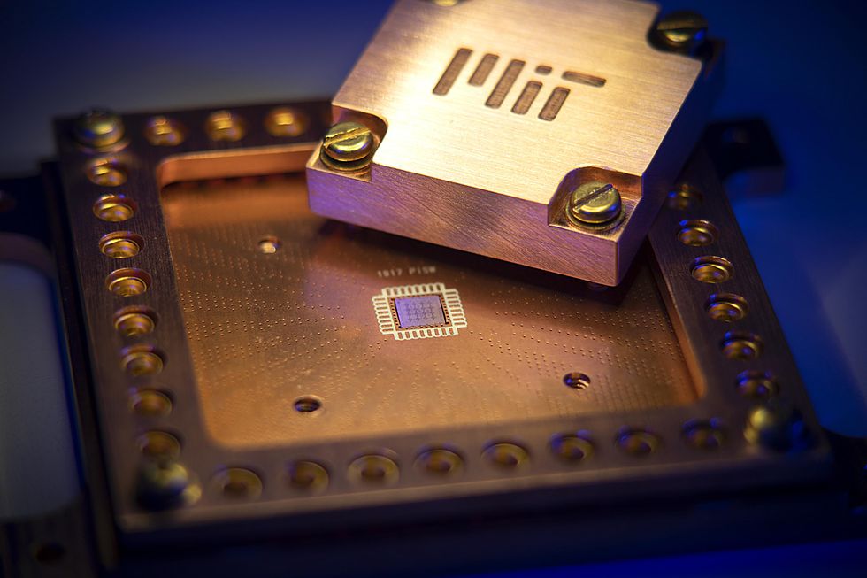
Quantum computing is a devilishly complex technology, with many technical hurdles impacting its development. Of these challenges two critical issues stand out: miniaturization and qubit quality.
IBM has adopted the superconducting qubit road map of reaching a 1,121-qubit processor by 2023, leading to the expectation that 1,000 qubits with today’s qubit form factor is feasible. However, current approaches will require very large chips (50 millimeters on a side, or larger) at the scale of small wafers, or the use of chiplets on multichip modules. While this approach will work, the aim is to attain a better path toward scalability.
Now researchers at MIT have been able to both reduce the size of the qubits and done so in a way that reduces the interference that occurs between neighboring qubits. The MIT researchers have increased the number of superconducting qubits that can be added onto a device by a factor of 100.
“We are addressing both qubit miniaturization and quality,” said William Oliver, the director for the Center for Quantum Engineering at MIT. “Unlike conventional transistor scaling, where only the number really matters, for qubits, large numbers are not sufficient, they must also be high-performance. Sacrificing performance for qubit number is not a useful trade in quantum computing. They must go hand in hand.”
The key to this big increase in qubit density and reduction of interference comes down to the use of two-dimensional materials, in particular the 2D insulator hexagonal boron nitride (hBN). The MIT researchers demonstrated that a few atomic monolayers of hBN can be stacked to form the insulator in the capacitors of a superconducting qubit.
Just like other capacitors, the capacitors in these superconducting circuits take the form of a sandwich in which an insulator material is sandwiched between two metal plates. The big difference for these capacitors is that the superconducting circuits can operate only at extremely low temperatures—less than 0.02 degrees above absolute zero (-273.15 °C).
 Superconducting qubits are measured at temperatures as low as 20 millikelvin in a dilution refrigerator.Nathan Fiske/MIT
In that environment, insulating materials that are available for the job, such as PE-CVD silicon oxide or silicon nitride, have quite a few defects that are too lossy for quantum computing applications. To get around these material shortcomings, most superconducting circuits use what are called coplanar capacitors. In these capacitors, the plates are positioned laterally to one another, rather than on top of one another.
As a result, the intrinsic silicon substrate below the plates and to a smaller degree the vacuum above the plates serve as the capacitor dielectric. Intrinsic silicon is chemically pure and therefore has few defects, and the large size dilutes the electric field at the plate interfaces, all of which leads to a low-loss capacitor. The lateral size of each plate in this open-face design ends up being quite large (typically 100 by 100 micrometers) in order to achieve the required capacitance.
In an effort to move away from the large lateral configuration, the MIT researchers embarked on a search for an insulator that has very few defects and is compatible with superconducting capacitor plates.
“We chose to study hBN because it is the most widely used insulator in 2D material research due to its cleanliness and chemical inertness,” said colead author Joel Wang, a research scientist in the Engineering Quantum Systems group of the MIT Research Laboratory for Electronics.
On either side of the hBN, the MIT researchers used the 2D superconducting material, niobium diselenide. One of the trickiest aspects of fabricating the capacitors was working with the niobium diselenide, which oxidizes in seconds when exposed to air, according to Wang. This necessitates that the assembly of the capacitor occur in a glove box filled with argon gas.
While this would seemingly complicate the scaling up of the production of these capacitors, Wang doesn’t regard this as a limiting factor.
“What determines the quality factor of the capacitor are the two interfaces between the two materials,” said Wang. “Once the sandwich is made, the two interfaces are “sealed” and we don’t see any noticeable degradation over time when exposed to the atmosphere.”
This lack of degradation is because around 90 percent of the electric field is contained within the sandwich structure, so the oxidation of the outer surface of the niobium diselenide does not play a significant role anymore. This ultimately makes the capacitor footprint much smaller, and it accounts for the reduction in cross talk between the neighboring qubits.
“The main challenge for scaling up the fabrication will be the wafer-scale growth of hBN and 2D superconductors like [niobium diselenide], and how one can do wafer-scale stacking of these films,” added Wang.
Wang believes that this research has shown 2D hBN to be a good insulator candidate for superconducting qubits. He says that the groundwork the MIT team has done will serve as a road map for using other hybrid 2D materials to build superconducting circuits.